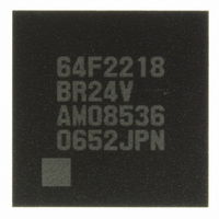
DF2218BR24V Renesas Electronics America, DF2218BR24V Datasheet - Page 598

DF2218BR24V
Manufacturer Part Number
DF2218BR24V
Description
IC H8S/2218 MCU FLASH 112-LFBGA
Manufacturer
Renesas Electronics America
Series
H8® H8S/2200r
Specifications of DF2218BR24V
Core Processor
H8S/2000
Core Size
16-Bit
Speed
24MHz
Connectivity
SCI, SmartCard, USB
Peripherals
DMA, POR, PWM, WDT
Number Of I /o
69
Program Memory Size
128KB (128K x 8)
Program Memory Type
FLASH
Ram Size
12K x 8
Voltage - Supply (vcc/vdd)
2.7 V ~ 3.6 V
Data Converters
A/D 6x10b
Oscillator Type
External
Operating Temperature
-20°C ~ 75°C
Package / Case
112-LFBGA
For Use With
HS0005KCU11H - EMULATOR E10A-USB H8S(X),SH2(A)3DK2218-SS - KIT DEV H8S/2218 WINDOWS SIDESHW3DK2218 - DEV EVAL KIT H8S/2218
Lead Free Status / RoHS Status
Lead free / RoHS Compliant
Eeprom Size
-
Available stocks
Company
Part Number
Manufacturer
Quantity
Price
Company:
Part Number:
DF2218BR24V
Manufacturer:
Renesas Electronics America
Quantity:
10 000
- Current page: 598 of 758
- Download datasheet (5Mb)
15.5
The A/D converter operates by successive approximation with 10-bit resolution. It has two
operating modes; single mode and scan mode. When changing the operating mode or analog input
channel, in order to prevent incorrect operation, first clear the bit ADST to 0 in ADCSR. The
ADST bit can be set at the same time as the operating mode or analog input channel is changed.
15.5.1
In single mode, A/D conversion is to be performed only once on the specified single channel. The
operations are as follows.
1. A/D conversion is started when the ADST bit is set to 1, according to software or external
2. When A/D conversion is completed, the result is transferred to the corresponding A/D data
3. On completion of conversion, the ADF bit in ADCSR is set to 1. If the ADIE bit is set to 1 at
4. The ADST bit remains set to 1 during A/D conversion. When A/D conversion ends, the ADST
Rev.7.00 Dec. 24, 2008 Page 542 of 698
REJ09B0074-0700
State of channel 0 (AN0)
State of channel 1 (AN1)
State of channel 2 (AN2)
State of channel 3 (AN3)
trigger input.
register to the channel.
this time, an ADI interrupt request is generated.
bit is automatically cleared to 0 and the A/D converter enters the wait state.
Figure 15.3 A/D Conversion Timing (Single-Chip Mode, Channel 1 Selected)
Single Mode
Operation
ADIE
ADST
ADF
ADDRA
ADDRB
ADDRC
ADDRD
Note: * Vertical arrows ( ) indicate instructions executed by software.
A/D
conversion
starts
Idle
Idle
Idle
Idle
A/D conversion
Set*
Set*
1
Idle
Clear*
Read conversion result*
A/D conversion result 1
A/D conversion
Set*
2
Read conversion result*
A/D conversion result 2
Clear*
Idle
Related parts for DF2218BR24V
Image
Part Number
Description
Manufacturer
Datasheet
Request
R

Part Number:
Description:
CONN SOCKET 2POS 7.92MM WHITE
Manufacturer:
Hirose Electric Co Ltd
Datasheet:

Part Number:
Description:
CONN SOCKET 4POS 7.92MM WHITE
Manufacturer:
Hirose Electric Co Ltd
Datasheet:

Part Number:
Description:
CONN SOCKET 5POS 7.92MM WHITE
Manufacturer:
Hirose Electric Co Ltd
Datasheet:

Part Number:
Description:
CONN SOCKET 3POS 7.92MM WHITE
Manufacturer:
Hirose Electric Co Ltd
Datasheet:

Part Number:
Description:
CONN SOCKET 5POS 7.92MM WHITE
Manufacturer:
Hirose Electric Co Ltd
Datasheet:

Part Number:
Description:
CONN SOCKET 2POS 7.92MM WHITE
Manufacturer:
Hirose Electric Co Ltd
Datasheet:

Part Number:
Description:
CONN SOCKET 3POS 7.92MM WHITE
Manufacturer:
Hirose Electric Co Ltd
Datasheet:

Part Number:
Description:
CONN SOCKET 4POS 7.92MM WHITE
Manufacturer:
Hirose Electric Co Ltd
Datasheet:

Part Number:
Description:
CONN HEADER 2POS 7.92MM R/A TIN
Manufacturer:
Hirose Electric Co Ltd
Datasheet:

Part Number:
Description:
CONN HEADER 4POS 7.92MM R/A TIN
Manufacturer:
Hirose Electric Co Ltd
Datasheet:

Part Number:
Description:
KIT STARTER FOR M16C/29
Manufacturer:
Renesas Electronics America
Datasheet:

Part Number:
Description:
KIT STARTER FOR R8C/2D
Manufacturer:
Renesas Electronics America
Datasheet:

Part Number:
Description:
R0K33062P STARTER KIT
Manufacturer:
Renesas Electronics America
Datasheet:

Part Number:
Description:
KIT STARTER FOR R8C/23 E8A
Manufacturer:
Renesas Electronics America
Datasheet:

Part Number:
Description:
KIT STARTER FOR R8C/25
Manufacturer:
Renesas Electronics America
Datasheet:


