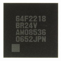
DF2218BR24V Renesas Electronics America, DF2218BR24V Datasheet - Page 43

DF2218BR24V
Manufacturer Part Number
DF2218BR24V
Description
IC H8S/2218 MCU FLASH 112-LFBGA
Manufacturer
Renesas Electronics America
Series
H8® H8S/2200r
Specifications of DF2218BR24V
Core Processor
H8S/2000
Core Size
16-Bit
Speed
24MHz
Connectivity
SCI, SmartCard, USB
Peripherals
DMA, POR, PWM, WDT
Number Of I /o
69
Program Memory Size
128KB (128K x 8)
Program Memory Type
FLASH
Ram Size
12K x 8
Voltage - Supply (vcc/vdd)
2.7 V ~ 3.6 V
Data Converters
A/D 6x10b
Oscillator Type
External
Operating Temperature
-20°C ~ 75°C
Package / Case
112-LFBGA
For Use With
HS0005KCU11H - EMULATOR E10A-USB H8S(X),SH2(A)3DK2218-SS - KIT DEV H8S/2218 WINDOWS SIDESHW3DK2218 - DEV EVAL KIT H8S/2218
Lead Free Status / RoHS Status
Lead free / RoHS Compliant
Eeprom Size
-
Available stocks
Company
Part Number
Manufacturer
Quantity
Price
Company:
Part Number:
DF2218BR24V
Manufacturer:
Renesas Electronics America
Quantity:
10 000
- Current page: 43 of 758
- Download datasheet (5Mb)
Figure 9.41 TCIU Interrupt Setting Timing............................................................................... 329
Figure 9.42 Timing for Status Flag Clearing by CPU ............................................................... 330
Figure 9.43 Timing for Status Flag Clearing by DMAC Activation ......................................... 330
Figure 9.44 Phase Difference, Overlap, and Pulse Width in Phase Counting Mode ................. 331
Figure 9.45 Contention between TCNT Write and Clear Operations........................................ 332
Figure 9.46 Contention between TCNT Write and Increment Operations ................................ 332
Figure 9.47 Contention between TGR Write and Compare Match............................................ 333
Figure 9.48 Contention between Buffer Register Write and Compare Match........................... 334
Figure 9.49 Contention between TGR Read and Input Capture ................................................ 334
Figure 9.50 Contention between TGR Write and Input Capture ............................................... 335
Figure 9.51 Contention between Buffer Register Write and Input Capture............................... 336
Figure 9.52 Contention between Overflow and Counter Clearing ............................................ 336
Figure 9.53 Contention between TCNT Write and Overflow.................................................... 337
Section 10 Watchdog Timer (WDT)
Figure 10.1 Block Diagram of WDT ......................................................................................... 340
Figure 10.2 Operation in Watchdog Timer Mode...................................................................... 343
Figure 10.3 Timing of WOVF Setting....................................................................................... 344
Figure 10.4 Operation in Interval Timer Mode ......................................................................... 344
Figure 10.5 Timing of OVF Setting........................................................................................... 345
Figure 10.6 Format of Data Written to TCNT and TCSR ......................................................... 346
Figure 10.7 Format of Data Written to RSTCSR (Example of WDT0) .................................... 347
Figure 10.8 Contention between TCNT Write and Increment................................................... 347
Section 11 Realtime Clock (RTC)
Figure 11.1 Block Diagram of RTC .......................................................................................... 349
Figure 11.2 Definition of Time Expression ............................................................................... 354
Figure 11.3 Initial Setting Procedure......................................................................................... 358
Figure 11.4 Example: Reading of Inaccurate Time Data........................................................... 359
Figure 11.5 Initializing Procedure in Using RTC Interrupt ....................................................... 361
Figure 11.6 Example of RTC Interrupt Handling Routine ........................................................ 361
Section 12 Serial Communication Interface
Figure 12.1 Block Diagram of SCI_0........................................................................................ 365
Figure 12.2 Block Diagram of SCI_2........................................................................................ 366
Figure 12.3 Examples of Base Clock when Average Transfer Rate Is Selected (1) .................. 388
Figure 12.3 Examples of Base Clock when Average Transfer Rate Is Selected (2) .................. 389
Figure 12.3 Examples of Base Clock when Average Transfer Rate Is Selected (3) .................. 390
Figure 12.4 Example of Average Transfer Rate Setting when TPU Clock Is Input (1)............ 391
Figure 12.4 Example of Average Transfer Rate Setting when TPU Clock Is Input (2)............ 392
Figure 12.4 Example of Average Transfer Rate Setting when TPU Clock Is Input (3)............ 393
Rev.7.00 Dec. 24, 2008 Page xli of liv
REJ09B0074-0700
Related parts for DF2218BR24V
Image
Part Number
Description
Manufacturer
Datasheet
Request
R

Part Number:
Description:
CONN SOCKET 2POS 7.92MM WHITE
Manufacturer:
Hirose Electric Co Ltd
Datasheet:

Part Number:
Description:
CONN SOCKET 4POS 7.92MM WHITE
Manufacturer:
Hirose Electric Co Ltd
Datasheet:

Part Number:
Description:
CONN SOCKET 5POS 7.92MM WHITE
Manufacturer:
Hirose Electric Co Ltd
Datasheet:

Part Number:
Description:
CONN SOCKET 3POS 7.92MM WHITE
Manufacturer:
Hirose Electric Co Ltd
Datasheet:

Part Number:
Description:
CONN SOCKET 5POS 7.92MM WHITE
Manufacturer:
Hirose Electric Co Ltd
Datasheet:

Part Number:
Description:
CONN SOCKET 2POS 7.92MM WHITE
Manufacturer:
Hirose Electric Co Ltd
Datasheet:

Part Number:
Description:
CONN SOCKET 3POS 7.92MM WHITE
Manufacturer:
Hirose Electric Co Ltd
Datasheet:

Part Number:
Description:
CONN SOCKET 4POS 7.92MM WHITE
Manufacturer:
Hirose Electric Co Ltd
Datasheet:

Part Number:
Description:
CONN HEADER 2POS 7.92MM R/A TIN
Manufacturer:
Hirose Electric Co Ltd
Datasheet:

Part Number:
Description:
CONN HEADER 4POS 7.92MM R/A TIN
Manufacturer:
Hirose Electric Co Ltd
Datasheet:

Part Number:
Description:
KIT STARTER FOR M16C/29
Manufacturer:
Renesas Electronics America
Datasheet:

Part Number:
Description:
KIT STARTER FOR R8C/2D
Manufacturer:
Renesas Electronics America
Datasheet:

Part Number:
Description:
R0K33062P STARTER KIT
Manufacturer:
Renesas Electronics America
Datasheet:

Part Number:
Description:
KIT STARTER FOR R8C/23 E8A
Manufacturer:
Renesas Electronics America
Datasheet:

Part Number:
Description:
KIT STARTER FOR R8C/25
Manufacturer:
Renesas Electronics America
Datasheet:


