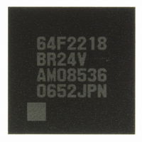
DF2218BR24V Renesas Electronics America, DF2218BR24V Datasheet - Page 494

DF2218BR24V
Manufacturer Part Number
DF2218BR24V
Description
IC H8S/2218 MCU FLASH 112-LFBGA
Manufacturer
Renesas Electronics America
Series
H8® H8S/2200r
Specifications of DF2218BR24V
Core Processor
H8S/2000
Core Size
16-Bit
Speed
24MHz
Connectivity
SCI, SmartCard, USB
Peripherals
DMA, POR, PWM, WDT
Number Of I /o
69
Program Memory Size
128KB (128K x 8)
Program Memory Type
FLASH
Ram Size
12K x 8
Voltage - Supply (vcc/vdd)
2.7 V ~ 3.6 V
Data Converters
A/D 6x10b
Oscillator Type
External
Operating Temperature
-20°C ~ 75°C
Package / Case
112-LFBGA
For Use With
HS0005KCU11H - EMULATOR E10A-USB H8S(X),SH2(A)3DK2218-SS - KIT DEV H8S/2218 WINDOWS SIDESHW3DK2218 - DEV EVAL KIT H8S/2218
Lead Free Status / RoHS Status
Lead free / RoHS Compliant
Eeprom Size
-
Available stocks
Company
Part Number
Manufacturer
Quantity
Price
Company:
Part Number:
DF2218BR24V
Manufacturer:
Renesas Electronics America
Quantity:
10 000
- Current page: 494 of 758
- Download datasheet (5Mb)
12.8
The SCI_0 supports the SCI select function which allows clock synchronous communication
between master LSI and one of multiple slave LSI. Figure 12.36 shows an example of
communication using the SCI select function. Figure 12.37 shows the operation.
The master LSI can communicate with slave LSI_A by bringing SEL_A and SEL_B signals low
and high, respectively. In this case, the TxD0_B pin of the slave LSI_B is brought high-
impedance state and the internal SCK0_A signal is fixed high. This halts the communication
operation of slave LSI_B. The master LSI can communicate with slave LSI_B by bringing the
SEL_A and SEL_B signals high and low, respectively.
The slave LSI detects the selection by receiving the low level input from the IRQ7 pin and
immediately executes data transmission/reception processing.
Note: The selection signals (SEL_A and SEL_B) of the LSI must be switched while the serial
Rev.7.00 Dec. 24, 2008 Page 438 of 698
REJ09B0074-0700
clock (M_SCK) is high after the end bit of the transmit data has been send. Note that one
selection signal can be brought low at the same time.
SCI Select Function (Clocked Synchronous Mode)
Figure 12.36 Example of Communication Using the SCI Select Function
Master LSI
M_SCK
M_RxD
M_TxD
SEL_A
SEL_B
IRQ7_A
RxD0_A
TxD0_A
IRQ7_B
RxD0_B
TxD0_B
SCK0
SCK0
Slave LSI_B (This LSI)
Slave LSI_A (This LSI)
C/A = CKE1 = SSE = 1
SCK0_B
SCK0_A
RSR0_A
controller
Transmission/
Interrupt
reception
TSR0_A
control
Related parts for DF2218BR24V
Image
Part Number
Description
Manufacturer
Datasheet
Request
R

Part Number:
Description:
CONN SOCKET 2POS 7.92MM WHITE
Manufacturer:
Hirose Electric Co Ltd
Datasheet:

Part Number:
Description:
CONN SOCKET 4POS 7.92MM WHITE
Manufacturer:
Hirose Electric Co Ltd
Datasheet:

Part Number:
Description:
CONN SOCKET 5POS 7.92MM WHITE
Manufacturer:
Hirose Electric Co Ltd
Datasheet:

Part Number:
Description:
CONN SOCKET 3POS 7.92MM WHITE
Manufacturer:
Hirose Electric Co Ltd
Datasheet:

Part Number:
Description:
CONN SOCKET 5POS 7.92MM WHITE
Manufacturer:
Hirose Electric Co Ltd
Datasheet:

Part Number:
Description:
CONN SOCKET 2POS 7.92MM WHITE
Manufacturer:
Hirose Electric Co Ltd
Datasheet:

Part Number:
Description:
CONN SOCKET 3POS 7.92MM WHITE
Manufacturer:
Hirose Electric Co Ltd
Datasheet:

Part Number:
Description:
CONN SOCKET 4POS 7.92MM WHITE
Manufacturer:
Hirose Electric Co Ltd
Datasheet:

Part Number:
Description:
CONN HEADER 2POS 7.92MM R/A TIN
Manufacturer:
Hirose Electric Co Ltd
Datasheet:

Part Number:
Description:
CONN HEADER 4POS 7.92MM R/A TIN
Manufacturer:
Hirose Electric Co Ltd
Datasheet:

Part Number:
Description:
KIT STARTER FOR M16C/29
Manufacturer:
Renesas Electronics America
Datasheet:

Part Number:
Description:
KIT STARTER FOR R8C/2D
Manufacturer:
Renesas Electronics America
Datasheet:

Part Number:
Description:
R0K33062P STARTER KIT
Manufacturer:
Renesas Electronics America
Datasheet:

Part Number:
Description:
KIT STARTER FOR R8C/23 E8A
Manufacturer:
Renesas Electronics America
Datasheet:

Part Number:
Description:
KIT STARTER FOR R8C/25
Manufacturer:
Renesas Electronics America
Datasheet:


