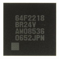
DF2218BR24V Renesas Electronics America, DF2218BR24V Datasheet - Page 739

DF2218BR24V
Manufacturer Part Number
DF2218BR24V
Description
IC H8S/2218 MCU FLASH 112-LFBGA
Manufacturer
Renesas Electronics America
Series
H8® H8S/2200r
Specifications of DF2218BR24V
Core Processor
H8S/2000
Core Size
16-Bit
Speed
24MHz
Connectivity
SCI, SmartCard, USB
Peripherals
DMA, POR, PWM, WDT
Number Of I /o
69
Program Memory Size
128KB (128K x 8)
Program Memory Type
FLASH
Ram Size
12K x 8
Voltage - Supply (vcc/vdd)
2.7 V ~ 3.6 V
Data Converters
A/D 6x10b
Oscillator Type
External
Operating Temperature
-20°C ~ 75°C
Package / Case
112-LFBGA
For Use With
HS0005KCU11H - EMULATOR E10A-USB H8S(X),SH2(A)3DK2218-SS - KIT DEV H8S/2218 WINDOWS SIDESHW3DK2218 - DEV EVAL KIT H8S/2218
Lead Free Status / RoHS Status
Lead free / RoHS Compliant
Eeprom Size
-
Available stocks
Company
Part Number
Manufacturer
Quantity
Price
Company:
Part Number:
DF2218BR24V
Manufacturer:
Renesas Electronics America
Quantity:
10 000
- Current page: 739 of 758
- Download datasheet (5Mb)
22.7
Table 22.10 lists the flash memory characteristics.
Table 22.10 Flash Memory Characteristics
Conditions: V
Item
Programming time*
Erase time*
Reprogramming count
Data retention time*
Programming Wait time after PSU1 bit setting*
Common
Erase
Notes: 1. Make each time setting in accordance with the program/program-verify flowchart or
2. Programming time per 128 bytes (Shows the total period for which the P-bit in the flash
Flash Memory Characteristics
1
*
erase/erase-verify flowchart.
memory control register (FLMCR1) is set. It does not include the programming
verification time.)
3
V
T
*
Wait time after P1 bit setting*
Wait time after P1 bit clear*
Wait time after PSU1 bit clear*
Wait time after PV1 bit setting*
Wait time after H’FF dummy write*
Wait time after PV1 bit clear*
Maximum programming count*
Wait time after SWE1 bit setting*
Wait time after SWE1 bit clear*
Wait time after ESU1 bit setting*
Wait time after E1 bit setting*
Wait time after E1 bit clear*
Wait time after ESU1 bit clear*
Wait time after EV1 bit setting*
Wait time after H'FF dummy write*
Wait time after EV1 bit clear*
Maximum erase count*
5
a
CC
SS
= –20 to +75°C (Programming/erasing operating temperature range)
1
= PLLV
8
= PLLV
*
2
*
4
SS
CC
= DrV
= DrV
1
SS
CC
*
5
= 0 V,
= 3.0 V to 3.6 V, Vref = 2.7 V to V
1
1
1
1
1
1
*
*
1
1
1
1
1
1
4
5
*
1
1
1
4
1
1
Symbol
t
t
N
t
y
z0
z1
z2
α
β
γ
ε
η
N1
N2
x
θ
y
z
α
β
γ
ε
η
N
P
E
DRP
WEC
Rev.7.00 Dec. 24, 2008 Page 683 of 698
Min.
—
—
100*
10
50
28
198
8
5
5
4
2
2
—
—
1
100
100
10
10
10
20
2
4
—
6
Typ.
10
50
10000*
—
50
30
200
10
5
5
4
2
2
—
—
1
100
100
10
10
10
20
2
4
—
7
CC
,
Max.
200
1000
—
—
—
32
202
12
—
—
—
—
—
6*
994*
—
—
—
100
—
—
—
—
—
100
4
REJ09B0074-0700
4
Unit
ms/128 bytes
ms/block
Times
Years
µs
µs
µs
µs
µs
µs
µs
µs
µs
Times
Times
µs
µs
µs
ms
µs
µs
µs
µs
µs
Times
Related parts for DF2218BR24V
Image
Part Number
Description
Manufacturer
Datasheet
Request
R

Part Number:
Description:
CONN SOCKET 2POS 7.92MM WHITE
Manufacturer:
Hirose Electric Co Ltd
Datasheet:

Part Number:
Description:
CONN SOCKET 4POS 7.92MM WHITE
Manufacturer:
Hirose Electric Co Ltd
Datasheet:

Part Number:
Description:
CONN SOCKET 5POS 7.92MM WHITE
Manufacturer:
Hirose Electric Co Ltd
Datasheet:

Part Number:
Description:
CONN SOCKET 3POS 7.92MM WHITE
Manufacturer:
Hirose Electric Co Ltd
Datasheet:

Part Number:
Description:
CONN SOCKET 5POS 7.92MM WHITE
Manufacturer:
Hirose Electric Co Ltd
Datasheet:

Part Number:
Description:
CONN SOCKET 2POS 7.92MM WHITE
Manufacturer:
Hirose Electric Co Ltd
Datasheet:

Part Number:
Description:
CONN SOCKET 3POS 7.92MM WHITE
Manufacturer:
Hirose Electric Co Ltd
Datasheet:

Part Number:
Description:
CONN SOCKET 4POS 7.92MM WHITE
Manufacturer:
Hirose Electric Co Ltd
Datasheet:

Part Number:
Description:
CONN HEADER 2POS 7.92MM R/A TIN
Manufacturer:
Hirose Electric Co Ltd
Datasheet:

Part Number:
Description:
CONN HEADER 4POS 7.92MM R/A TIN
Manufacturer:
Hirose Electric Co Ltd
Datasheet:

Part Number:
Description:
KIT STARTER FOR M16C/29
Manufacturer:
Renesas Electronics America
Datasheet:

Part Number:
Description:
KIT STARTER FOR R8C/2D
Manufacturer:
Renesas Electronics America
Datasheet:

Part Number:
Description:
R0K33062P STARTER KIT
Manufacturer:
Renesas Electronics America
Datasheet:

Part Number:
Description:
KIT STARTER FOR R8C/23 E8A
Manufacturer:
Renesas Electronics America
Datasheet:

Part Number:
Description:
KIT STARTER FOR R8C/25
Manufacturer:
Renesas Electronics America
Datasheet:


