DF2218BR24V Renesas Electronics America, DF2218BR24V Datasheet - Page 39
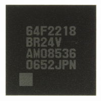
DF2218BR24V
Manufacturer Part Number
DF2218BR24V
Description
IC H8S/2218 MCU FLASH 112-LFBGA
Manufacturer
Renesas Electronics America
Series
H8® H8S/2200r
Specifications of DF2218BR24V
Core Processor
H8S/2000
Core Size
16-Bit
Speed
24MHz
Connectivity
SCI, SmartCard, USB
Peripherals
DMA, POR, PWM, WDT
Number Of I /o
69
Program Memory Size
128KB (128K x 8)
Program Memory Type
FLASH
Ram Size
12K x 8
Voltage - Supply (vcc/vdd)
2.7 V ~ 3.6 V
Data Converters
A/D 6x10b
Oscillator Type
External
Operating Temperature
-20°C ~ 75°C
Package / Case
112-LFBGA
For Use With
HS0005KCU11H - EMULATOR E10A-USB H8S(X),SH2(A)3DK2218-SS - KIT DEV H8S/2218 WINDOWS SIDESHW3DK2218 - DEV EVAL KIT H8S/2218
Lead Free Status / RoHS Status
Lead free / RoHS Compliant
Eeprom Size
-
Available stocks
Company
Part Number
Manufacturer
Quantity
Price
Company:

Part Number:
DF2218BR24V
Manufacturer:
Renesas Electronics America
Quantity:
10 000


Section 1 Overview
Figure 1.1
Figure 1.2
Figure 1.3
Figure 1.4
Figure 1.5
Figure 1.6
Figure 1.7
Figure 1.8
Figure 1.9
Figure 1.10 Pin Arrangements of HD6432211, HD6432210 and HD6432210S
Figure 1.11 Pin Arrangements of HD64F2212, HD64F2212U, HD64F2212CU, HD64F2211,
Figure 1.12 Pin Arrangements of HD6432211, HD6432210 and HD6432210S
Section 2 CPU
Figure 2.1
Figure 2.2
Figure 2.3
Figure 2.4
Figure 2.5
Figure 2.6
Figure 2.7
Figure 2.8
Figure 2.9
Figure 2.9
Figure 2.10 Memory Data Formats............................................................................................ 45
Figure 2.11 Instruction Formats (Examples) ............................................................................. 57
Figure 2.12 Branch Address Specification in Memory Indirect Mode ...................................... 61
Figure 2.13 State Transitions..................................................................................................... 65
Figure 2.14 Flowchart of Method for Accessing Registers Containing Write-Only Bits .......... 69
Internal Block Diagram of HD64F2218, HD64F2218U, HD64F2218CU and
HD642217CU.........................................................................................................
Internal Block Diagram of HD6432217 .................................................................
Internal Block Diagram of HD64F2212, HD64F2212U, HD64F2212CU,
HD64F2211, HD64F2211U, HD64F2211CU and HD64F2210CU.......................
Internal Block Diagram of HD6432211, HD6432210 and HD6432210S ..............
Pin Arrangements of HD64F2218, HD64F2218U, HD64F2218CU and
HD64F2217CU (TFP-100G, TFP-100GV)............................................................
Pin Arrangements of HD64F2218, HD64F2218U, HD64F2218CU and
HD64F2217CU (BP-112, BP-112V)......................................................................
Pin Arrangements of HD6432217 (TFP-100G, TFP-100GV)................................
Pin Arrangements of HD6432217 (BP-112, BP-112V) ......................................... 10
Pin Arrangements of HD64F2212, HD64F2212U, HD64F2212CU, HD64F2211,
HD64F2211U, HD64F2211CU and HD64F2210CU (FP-64E, FP-64EV)............ 11
(FP-64E, FP-64EV) ................................................................................................ 12
HD64F2211U, HD64F2211CU and HD64F2210CU (TNP-64B, TNP-64BV) ..... 13
(TNP-64B, TNP-64BV) ......................................................................................... 14
Exception Vector Table (Normal Mode)................................................................ 35
Stack Structure in Normal Mode............................................................................ 35
Exception Vector Table (Advanced Mode)............................................................ 36
Stack Structure in Advanced Mode ........................................................................ 37
Memory Map.......................................................................................................... 38
CPU Registers ........................................................................................................ 39
Usage of General Registers .................................................................................... 40
Stack....................................................................................................................... 41
General Register Data Formats (1)......................................................................... 44
General Register Data Formats (2)......................................................................... 44
Figures
Rev.7.00 Dec. 24, 2008 Page xxxvii of liv
REJ09B0074-0700
3
4
5
6
7
8
9
Related parts for DF2218BR24V
Image
Part Number
Description
Manufacturer
Datasheet
Request
R

Part Number:
Description:
CONN SOCKET 2POS 7.92MM WHITE
Manufacturer:
Hirose Electric Co Ltd
Datasheet:

Part Number:
Description:
CONN SOCKET 4POS 7.92MM WHITE
Manufacturer:
Hirose Electric Co Ltd
Datasheet:

Part Number:
Description:
CONN SOCKET 5POS 7.92MM WHITE
Manufacturer:
Hirose Electric Co Ltd
Datasheet:

Part Number:
Description:
CONN SOCKET 3POS 7.92MM WHITE
Manufacturer:
Hirose Electric Co Ltd
Datasheet:
Part Number:
Description:
CONN SOCKET 5POS 7.92MM WHITE
Manufacturer:
Hirose Electric Co Ltd
Datasheet:

Part Number:
Description:
CONN SOCKET 2POS 7.92MM WHITE
Manufacturer:
Hirose Electric Co Ltd
Datasheet:
Part Number:
Description:
CONN SOCKET 3POS 7.92MM WHITE
Manufacturer:
Hirose Electric Co Ltd
Datasheet:
Part Number:
Description:
CONN SOCKET 4POS 7.92MM WHITE
Manufacturer:
Hirose Electric Co Ltd
Datasheet:

Part Number:
Description:
CONN HEADER 2POS 7.92MM R/A TIN
Manufacturer:
Hirose Electric Co Ltd
Datasheet:

Part Number:
Description:
CONN HEADER 4POS 7.92MM R/A TIN
Manufacturer:
Hirose Electric Co Ltd
Datasheet:

Part Number:
Description:
KIT STARTER FOR M16C/29
Manufacturer:
Renesas Electronics America
Datasheet:

Part Number:
Description:
KIT STARTER FOR R8C/2D
Manufacturer:
Renesas Electronics America
Datasheet:

Part Number:
Description:
R0K33062P STARTER KIT
Manufacturer:
Renesas Electronics America
Datasheet:

Part Number:
Description:
KIT STARTER FOR R8C/23 E8A
Manufacturer:
Renesas Electronics America
Datasheet:

Part Number:
Description:
KIT STARTER FOR R8C/25
Manufacturer:
Renesas Electronics America
Datasheet: