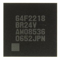
DF2218BR24V Renesas Electronics America, DF2218BR24V Datasheet - Page 586

DF2218BR24V
Manufacturer Part Number
DF2218BR24V
Description
IC H8S/2218 MCU FLASH 112-LFBGA
Manufacturer
Renesas Electronics America
Series
H8® H8S/2200r
Specifications of DF2218BR24V
Core Processor
H8S/2000
Core Size
16-Bit
Speed
24MHz
Connectivity
SCI, SmartCard, USB
Peripherals
DMA, POR, PWM, WDT
Number Of I /o
69
Program Memory Size
128KB (128K x 8)
Program Memory Type
FLASH
Ram Size
12K x 8
Voltage - Supply (vcc/vdd)
2.7 V ~ 3.6 V
Data Converters
A/D 6x10b
Oscillator Type
External
Operating Temperature
-20°C ~ 75°C
Package / Case
112-LFBGA
For Use With
HS0005KCU11H - EMULATOR E10A-USB H8S(X),SH2(A)3DK2218-SS - KIT DEV H8S/2218 WINDOWS SIDESHW3DK2218 - DEV EVAL KIT H8S/2218
Lead Free Status / RoHS Status
Lead free / RoHS Compliant
Eeprom Size
-
Available stocks
Company
Part Number
Manufacturer
Quantity
Price
Company:
Part Number:
DF2218BR24V
Manufacturer:
Renesas Electronics America
Quantity:
10 000
- Current page: 586 of 758
- Download datasheet (5Mb)
Section 14 Universal Serial Bus (USB)
14.8.10 Level Shifter for VBUS and IRQx Pins
The VBUS and IRQx pins of this USB module must be connected to the USB connector’s VBUS
pin via a level shifter. This is because the USB module has a circuit that operates by detecting
USB cable connection or disconnection.
Even if the power of the device incorporating this USB module is turned off, 5-V power is applied
to the USB connector’s VBUS pin while the USB cable is connected to the device set. To protect
the LSI from destruction, use a level shifter such as the HD74LV-A Series, which allows voltage
application to the pin even when the power is off.
14.8.11 USB Endpoint Data Read and Write
To write data to an USB endpoint data register (UEDR0i, UEDR1, or UEDR3) on the transmit side
using a CPU word or longword transfer instruction, the size of data to be written must be smaller
than the size of data that is to be transmitted.
For example, when 7-byte data is transferred to the host, 8-byte data is sent to the host if data is
written twice by the longword transfer instructions or if data is written four times by the word
transfer instructions. To write 7-byte data correctly, data must be written once by a longword
transfer instruction, once by a word transfer instruction, and once by a byte transfer instruction, or
data must be written three times by a word transfer instruction and once by a byte transfer
instruction.
To read data from the USB endpoint data register (UEDR0o or UEDR2) on the receive side, the
correct size of data must be read. In this case, the data size is specified by the USB endpoint
receive size register (UESZ0o or UESZ2).
To execute DMA transfer on data in the USB endpoint data register using the on-chip DMAC,
byte transfer musts be used. In word transfer, odd-byte data cannot be transferred. Word transfer is
thus disabled.
14.8.12 Restrictions on Entering and Canceling Power-Down Mode
Before entering the power-down mode, set the USB module stop 2 state. The UDC core must not
be reset.
To access the USB module after canceling power-down mode, cancel the USB module stop 2 state
and wait for the USB operating clock (48 MHz) stabilization time.
Rev.7.00 Dec. 24, 2008 Page 530 of 698
REJ09B0074-0700
Related parts for DF2218BR24V
Image
Part Number
Description
Manufacturer
Datasheet
Request
R

Part Number:
Description:
CONN SOCKET 2POS 7.92MM WHITE
Manufacturer:
Hirose Electric Co Ltd
Datasheet:

Part Number:
Description:
CONN SOCKET 4POS 7.92MM WHITE
Manufacturer:
Hirose Electric Co Ltd
Datasheet:

Part Number:
Description:
CONN SOCKET 5POS 7.92MM WHITE
Manufacturer:
Hirose Electric Co Ltd
Datasheet:

Part Number:
Description:
CONN SOCKET 3POS 7.92MM WHITE
Manufacturer:
Hirose Electric Co Ltd
Datasheet:

Part Number:
Description:
CONN SOCKET 5POS 7.92MM WHITE
Manufacturer:
Hirose Electric Co Ltd
Datasheet:

Part Number:
Description:
CONN SOCKET 2POS 7.92MM WHITE
Manufacturer:
Hirose Electric Co Ltd
Datasheet:

Part Number:
Description:
CONN SOCKET 3POS 7.92MM WHITE
Manufacturer:
Hirose Electric Co Ltd
Datasheet:

Part Number:
Description:
CONN SOCKET 4POS 7.92MM WHITE
Manufacturer:
Hirose Electric Co Ltd
Datasheet:

Part Number:
Description:
CONN HEADER 2POS 7.92MM R/A TIN
Manufacturer:
Hirose Electric Co Ltd
Datasheet:

Part Number:
Description:
CONN HEADER 4POS 7.92MM R/A TIN
Manufacturer:
Hirose Electric Co Ltd
Datasheet:

Part Number:
Description:
KIT STARTER FOR M16C/29
Manufacturer:
Renesas Electronics America
Datasheet:

Part Number:
Description:
KIT STARTER FOR R8C/2D
Manufacturer:
Renesas Electronics America
Datasheet:

Part Number:
Description:
R0K33062P STARTER KIT
Manufacturer:
Renesas Electronics America
Datasheet:

Part Number:
Description:
KIT STARTER FOR R8C/23 E8A
Manufacturer:
Renesas Electronics America
Datasheet:

Part Number:
Description:
KIT STARTER FOR R8C/25
Manufacturer:
Renesas Electronics America
Datasheet:


