YLCDRSK2378 Renesas Electronics America, YLCDRSK2378 Datasheet - Page 1023
YLCDRSK2378
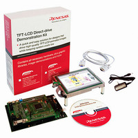
Manufacturer Part Number
YLCDRSK2378
Description
KIT DEV EVAL H8S/2378 LCD
Manufacturer
Renesas Electronics America
Series
H8®r
Datasheet
1.YR0K42378FC000BA.pdf
(1208 pages)
Specifications of YLCDRSK2378
Main Purpose
Displays, LCD Controller
Embedded
Yes, MCU, 16-Bit
Utilized Ic / Part
YLCDRSK2378
Primary Attributes
5.7" QVGA, Touch Screen
Secondary Attributes
Source Code on CD, Debugging Requires Emulator Cable E10A USB/JTAG
Lead Free Status / RoHS Status
Lead free / RoHS Compliant


This LSI has an on-chip clock pulse generator (CPG) that generates the system clock (
internal clocks.
The clock pulse generator consists of an oscillator circuit, PLL circuit, and divider.
Figure 23.1 shows a block diagram of the clock pulse generator.
The frequency can be changed by means of the PLL circuit. Frequency changes are made by
software by means of settings in the PLL control register (PLLCR) and the system clock control
register (SCKCR).
23.1
The clock pulse generator has the following registers.
• System clock control register (SCKCR)
• PLL control register (PLLCR)
23.1.1
SCKCR controls
used by the PLL circuit is changed, and the division ratio used by the divider.
CPG0400A_010020020400
Legend:
PLLCR: PLL system control register
SCKCR: System clock control register
EXTAL
XTAL
Register Descriptions
System Clock Control Register (SCKCR)
Oscillator
φ
clock output and selects operation when the frequency multiplication factor
Figure 23.1 Block Diagram of Clock Pulse Generator
Section 23 Clock Pulse Generator
PLL circuit
(×1, 2, 4)
PLLCR
STC0, STC1
Rev.7.00 Mar. 18, 2009 page 955 of 1136
Divider
SCKCR
SCK2 to SCK0
Section 23 Clock Pulse Generator
System clock
to φ pin
REJ09B0109-0700
Internal clock
to peripheral
modules
φ
) and
Related parts for YLCDRSK2378
Image
Part Number
Description
Manufacturer
Datasheet
Request
R

Part Number:
Description:
KIT STARTER FOR M16C/29
Manufacturer:
Renesas Electronics America
Datasheet:

Part Number:
Description:
KIT STARTER FOR R8C/2D
Manufacturer:
Renesas Electronics America
Datasheet:

Part Number:
Description:
R0K33062P STARTER KIT
Manufacturer:
Renesas Electronics America
Datasheet:

Part Number:
Description:
KIT STARTER FOR R8C/23 E8A
Manufacturer:
Renesas Electronics America
Datasheet:

Part Number:
Description:
KIT STARTER FOR R8C/25
Manufacturer:
Renesas Electronics America
Datasheet:

Part Number:
Description:
KIT STARTER H8S2456 SHARPE DSPLY
Manufacturer:
Renesas Electronics America
Datasheet:

Part Number:
Description:
KIT STARTER FOR R8C38C
Manufacturer:
Renesas Electronics America
Datasheet:

Part Number:
Description:
KIT STARTER FOR R8C35C
Manufacturer:
Renesas Electronics America
Datasheet:

Part Number:
Description:
KIT STARTER FOR R8CL3AC+LCD APPS
Manufacturer:
Renesas Electronics America
Datasheet:
Part Number:
Description:
KIT STARTER FOR RX610
Manufacturer:
Renesas Electronics America
Datasheet:

Part Number:
Description:
KIT STARTER FOR R32C/118
Manufacturer:
Renesas Electronics America
Datasheet:

Part Number:
Description:
KIT DEV RSK-R8C/26-29
Manufacturer:
Renesas Electronics America
Datasheet:

Part Number:
Description:
KIT STARTER FOR SH7124
Manufacturer:
Renesas Electronics America
Datasheet:

Part Number:
Description:
KIT STARTER FOR H8SX/1622
Manufacturer:
Renesas Electronics America
Datasheet:

Part Number:
Description:
KIT DEV FOR SH7203
Manufacturer:
Renesas Electronics America
Datasheet: