YLCDRSK2378 Renesas Electronics America, YLCDRSK2378 Datasheet - Page 917
YLCDRSK2378
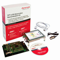
Manufacturer Part Number
YLCDRSK2378
Description
KIT DEV EVAL H8S/2378 LCD
Manufacturer
Renesas Electronics America
Series
H8®r
Datasheet
1.YR0K42378FC000BA.pdf
(1208 pages)
Specifications of YLCDRSK2378
Main Purpose
Displays, LCD Controller
Embedded
Yes, MCU, 16-Bit
Utilized Ic / Part
YLCDRSK2378
Primary Attributes
5.7" QVGA, Touch Screen
Secondary Attributes
Source Code on CD, Debugging Requires Emulator Cable E10A USB/JTAG
Lead Free Status / RoHS Status
Lead free / RoHS Compliant


Table 20.6 System Clock Frequencies for which Automatic Adjustment of LSI Bit Rate Is
Host Bit Rate
19,200 bps
9,600 bps
20.6.2
On-board programming/erasing of an individual flash memory block can also be performed in user
program mode by branching to a user program/erase program. The user must set branching
conditions and provide on-board means of supplying programming data. The flash memory must
contain the program/erase program or a program which provides the program/erase program from
external memory. Because the flash memory itself cannot be read during programming/erasing,
transfer the program/erase program to on-chip RAM, as like in boot mode. Figure 20.6 shows a
sample procedure for programming/erasing in user program mode. Prepare a program/erase
program in accordance with the description in section 20.7, Flash Memory Programming/Erasing.
Figure 20.6 Programming/Erasing Flowchart Example in User Program Mode
User Program Mode
Possible
program (flash memory programming)
Branch to user program/erase control
Transfer user program/erase control
Execute user program/erase control
Branch to flash memory application
program to RAM
program in RAM
Program/erase?
Reset-start
program
System Clock Frequency Range of LSI
8 to 25 MHz
8 to 25 MHz
Yes
No
Section 20 Flash Memory (0.35-μm F-ZTAT Version)
Branch to flash memory application
Rev.7.00 Mar. 18, 2009 page 849 of 1136
program
REJ09B0109-0700
Related parts for YLCDRSK2378
Image
Part Number
Description
Manufacturer
Datasheet
Request
R

Part Number:
Description:
KIT STARTER FOR M16C/29
Manufacturer:
Renesas Electronics America
Datasheet:

Part Number:
Description:
KIT STARTER FOR R8C/2D
Manufacturer:
Renesas Electronics America
Datasheet:

Part Number:
Description:
R0K33062P STARTER KIT
Manufacturer:
Renesas Electronics America
Datasheet:

Part Number:
Description:
KIT STARTER FOR R8C/23 E8A
Manufacturer:
Renesas Electronics America
Datasheet:

Part Number:
Description:
KIT STARTER FOR R8C/25
Manufacturer:
Renesas Electronics America
Datasheet:

Part Number:
Description:
KIT STARTER H8S2456 SHARPE DSPLY
Manufacturer:
Renesas Electronics America
Datasheet:

Part Number:
Description:
KIT STARTER FOR R8C38C
Manufacturer:
Renesas Electronics America
Datasheet:

Part Number:
Description:
KIT STARTER FOR R8C35C
Manufacturer:
Renesas Electronics America
Datasheet:

Part Number:
Description:
KIT STARTER FOR R8CL3AC+LCD APPS
Manufacturer:
Renesas Electronics America
Datasheet:
Part Number:
Description:
KIT STARTER FOR RX610
Manufacturer:
Renesas Electronics America
Datasheet:

Part Number:
Description:
KIT STARTER FOR R32C/118
Manufacturer:
Renesas Electronics America
Datasheet:

Part Number:
Description:
KIT DEV RSK-R8C/26-29
Manufacturer:
Renesas Electronics America
Datasheet:

Part Number:
Description:
KIT STARTER FOR SH7124
Manufacturer:
Renesas Electronics America
Datasheet:

Part Number:
Description:
KIT STARTER FOR H8SX/1622
Manufacturer:
Renesas Electronics America
Datasheet:

Part Number:
Description:
KIT DEV FOR SH7203
Manufacturer:
Renesas Electronics America
Datasheet: