YLCDRSK2378 Renesas Electronics America, YLCDRSK2378 Datasheet - Page 285
YLCDRSK2378
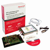
Manufacturer Part Number
YLCDRSK2378
Description
KIT DEV EVAL H8S/2378 LCD
Manufacturer
Renesas Electronics America
Series
H8®r
Datasheet
1.YR0K42378FC000BA.pdf
(1208 pages)
Specifications of YLCDRSK2378
Main Purpose
Displays, LCD Controller
Embedded
Yes, MCU, 16-Bit
Utilized Ic / Part
YLCDRSK2378
Primary Attributes
5.7" QVGA, Touch Screen
Secondary Attributes
Source Code on CD, Debugging Requires Emulator Cable E10A USB/JTAG
Lead Free Status / RoHS Status
Lead free / RoHS Compliant


Commands that are supported by this LSI are NOP, auto-refresh (REF), self-refresh (SELF), all
bank precharge (PALL), row address strobe bank-active (ACTV), read (READ), write (WRIT),
and mode-register write (MRS). Commands for bank control cannot be used.
6.7.2
With continuous synchronous DRAM space, the row address and column address are multiplexed.
In address multiplexing, the size of the shift of the row address is selected with bits MXC2 to
MXC0 in DRAMCR. The address-precharge-setting command (Precharge-sel) can be output on
the upper column address. Table 6.8 shows the relation between the settings of MXC2 to MXC0
and the shift size. The MXC2 bit should be set to 1 when the synchronous DRAM interface is
used.
Table 6.8
Legend:
×: Don’t care.
P: Precharge-sel
Row
address
Column
address
MXC2 MXC1 MXC0
Address Multiplexing
0
1
0
1
DRAMCR
Relation between Settings of Bits MXC2 to MXC0 and Address Multiplexing
×
×
0
1
0
1
×
×
0
1
0
1
0
1
0
1
Shift
8
bits
9
bits
10
bits
11
bits
Size A23 to
⎯
⎯
⎯
⎯
A16
A23 to
A16
A23 to
A16
A23 to
A16
A23 to
A16
A23 to
A16
A23 to
A16
A23 to
A16
A23 to
A16
A15 A14 A13 A12 A11 A10 A9 A8 A7 A6 A5 A4 A3 A2 A1 A0
A23 A22 A21 A20 A19 A18 A17 A16 A15 A14 A13 A12 A11 A10 A9 A8
A15 A23 A22 A21 A20 A19 A18 A17 A16 A15 A14 A13 A12 A11 A10 A9
A15 A14 A23 A22 A21 A20 A19 A18 A17 A16 A15 A14 A13 A12 A11 A10
A15 A14 A13 A23 A22 A21 A20 A19 A18 A17 A16 A15 A14 A13 A12 A11
P
P
P
P
P
P
P
P
P
P
P
P
P
P
P
P A11 A10 A9 A8 A7 A6 A5 A4 A3 A2 A1 A0
Reserved (setting prohibited)
Reserved (setting prohibited)
P
P
P A10 A9 A8 A7 A6 A5 A4 A3 A2 A1 A0
Rev.7.00 Mar. 18, 2009 page 217 of 1136
P
P
Address Pins
A9 A8 A7 A6 A5 A4 A3 A2 A1 A0
P
A8 A7 A6 A5 A4 A3 A2 A1 A0
Section 6 Bus Controller (BSC)
REJ09B0109-0700
Related parts for YLCDRSK2378
Image
Part Number
Description
Manufacturer
Datasheet
Request
R

Part Number:
Description:
KIT STARTER FOR M16C/29
Manufacturer:
Renesas Electronics America
Datasheet:

Part Number:
Description:
KIT STARTER FOR R8C/2D
Manufacturer:
Renesas Electronics America
Datasheet:

Part Number:
Description:
R0K33062P STARTER KIT
Manufacturer:
Renesas Electronics America
Datasheet:

Part Number:
Description:
KIT STARTER FOR R8C/23 E8A
Manufacturer:
Renesas Electronics America
Datasheet:

Part Number:
Description:
KIT STARTER FOR R8C/25
Manufacturer:
Renesas Electronics America
Datasheet:

Part Number:
Description:
KIT STARTER H8S2456 SHARPE DSPLY
Manufacturer:
Renesas Electronics America
Datasheet:

Part Number:
Description:
KIT STARTER FOR R8C38C
Manufacturer:
Renesas Electronics America
Datasheet:

Part Number:
Description:
KIT STARTER FOR R8C35C
Manufacturer:
Renesas Electronics America
Datasheet:

Part Number:
Description:
KIT STARTER FOR R8CL3AC+LCD APPS
Manufacturer:
Renesas Electronics America
Datasheet:
Part Number:
Description:
KIT STARTER FOR RX610
Manufacturer:
Renesas Electronics America
Datasheet:

Part Number:
Description:
KIT STARTER FOR R32C/118
Manufacturer:
Renesas Electronics America
Datasheet:

Part Number:
Description:
KIT DEV RSK-R8C/26-29
Manufacturer:
Renesas Electronics America
Datasheet:

Part Number:
Description:
KIT STARTER FOR SH7124
Manufacturer:
Renesas Electronics America
Datasheet:

Part Number:
Description:
KIT STARTER FOR H8SX/1622
Manufacturer:
Renesas Electronics America
Datasheet:

Part Number:
Description:
KIT DEV FOR SH7203
Manufacturer:
Renesas Electronics America
Datasheet: