YLCDRSK2378 Renesas Electronics America, YLCDRSK2378 Datasheet - Page 444
YLCDRSK2378
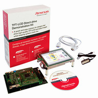
Manufacturer Part Number
YLCDRSK2378
Description
KIT DEV EVAL H8S/2378 LCD
Manufacturer
Renesas Electronics America
Series
H8®r
Datasheet
1.YR0K42378FC000BA.pdf
(1208 pages)
Specifications of YLCDRSK2378
Main Purpose
Displays, LCD Controller
Embedded
Yes, MCU, 16-Bit
Utilized Ic / Part
YLCDRSK2378
Primary Attributes
5.7" QVGA, Touch Screen
Secondary Attributes
Source Code on CD, Debugging Requires Emulator Cable E10A USB/JTAG
Lead Free Status / RoHS Status
Lead free / RoHS Compliant


Section 8 EXDMA Controller (EXDMAC)
Single Address Mode: In single address mode, the EDACK signal is used instead of the source or
destination address register to transfer data directly between an external device and external
memory. In this mode, the EXDMAC accesses the transfer source or transfer destination external
device by outputting the external I/O strobe signal (EDACK), and at the same time accesses the
other external device in the transfer by outputting an address. In this way, DMA transfer can be
executed in one bus cycle. In the example of transfer between external memory and an external
device with DACK shown in figure 8.3, data is output to the data bus by the external device and
written to external memory in the same bus cycle.
The transfer direction, that is whether the external device with DACK is the transfer source or
transfer destination, can be specified with the SDIR bit in EDMDR. Transfer is performed from
the external memory (EDSAR) to the external device with DACK when SDIR = 0, and from the
external device with DACK to the external memory (EDDAR) when SDIR = 1.
The setting in the source or destination address register not used in the transfer is ignored.
The EDACK pin becomes valid automatically when single address mode is selected. The EDACK
pin is active-low. ETEND pin output can be enabled or disabled by means of the ETENDE bit in
EDMDR. ETEND is output for one bus cycle.
Figure 8.3 shows the data flow in single address mode, and figure 8.4 shows an example of the
timing.
Rev.7.00 Mar. 18, 2009 page 376 of 1136
REJ09B0109-0700
φ
Address bus
RD
WR
ETEND
Figure 8.2 Example of Timing in Dual Address Mode
read cycle
EXDMA
EDSAR
write cycle
EXDMA
EDDAR
Related parts for YLCDRSK2378
Image
Part Number
Description
Manufacturer
Datasheet
Request
R

Part Number:
Description:
KIT STARTER FOR M16C/29
Manufacturer:
Renesas Electronics America
Datasheet:

Part Number:
Description:
KIT STARTER FOR R8C/2D
Manufacturer:
Renesas Electronics America
Datasheet:

Part Number:
Description:
R0K33062P STARTER KIT
Manufacturer:
Renesas Electronics America
Datasheet:

Part Number:
Description:
KIT STARTER FOR R8C/23 E8A
Manufacturer:
Renesas Electronics America
Datasheet:

Part Number:
Description:
KIT STARTER FOR R8C/25
Manufacturer:
Renesas Electronics America
Datasheet:

Part Number:
Description:
KIT STARTER H8S2456 SHARPE DSPLY
Manufacturer:
Renesas Electronics America
Datasheet:

Part Number:
Description:
KIT STARTER FOR R8C38C
Manufacturer:
Renesas Electronics America
Datasheet:

Part Number:
Description:
KIT STARTER FOR R8C35C
Manufacturer:
Renesas Electronics America
Datasheet:

Part Number:
Description:
KIT STARTER FOR R8CL3AC+LCD APPS
Manufacturer:
Renesas Electronics America
Datasheet:
Part Number:
Description:
KIT STARTER FOR RX610
Manufacturer:
Renesas Electronics America
Datasheet:

Part Number:
Description:
KIT STARTER FOR R32C/118
Manufacturer:
Renesas Electronics America
Datasheet:

Part Number:
Description:
KIT DEV RSK-R8C/26-29
Manufacturer:
Renesas Electronics America
Datasheet:

Part Number:
Description:
KIT STARTER FOR SH7124
Manufacturer:
Renesas Electronics America
Datasheet:

Part Number:
Description:
KIT STARTER FOR H8SX/1622
Manufacturer:
Renesas Electronics America
Datasheet:

Part Number:
Description:
KIT DEV FOR SH7203
Manufacturer:
Renesas Electronics America
Datasheet: