YLCDRSK2378 Renesas Electronics America, YLCDRSK2378 Datasheet - Page 765
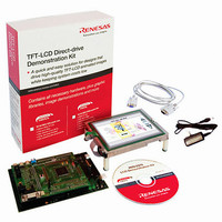
YLCDRSK2378
Manufacturer Part Number
YLCDRSK2378
Description
KIT DEV EVAL H8S/2378 LCD
Manufacturer
Renesas Electronics America
Series
H8®r
Datasheet
1.YR0K42378FC000BA.pdf
(1208 pages)
Specifications of YLCDRSK2378
Main Purpose
Displays, LCD Controller
Embedded
Yes, MCU, 16-Bit
Utilized Ic / Part
YLCDRSK2378
Primary Attributes
5.7" QVGA, Touch Screen
Secondary Attributes
Source Code on CD, Debugging Requires Emulator Cable E10A USB/JTAG
Lead Free Status / RoHS Status
Lead free / RoHS Compliant


Smart Card Interface Mode (When SMIF in SCMR is 1)
Bit
7
6
5
4
3
2
Bit Name
GM
BLK
PE
O/E
BCP1
BCP0
Initial Value
0
0
0
0
0
0
R/W
R/W
R/W
R/W
R/W
R/W
R/W
Section 15 Serial Communication Interface (SCI, IrDA)
Description
GSM Mode
When this bit is set to 1, the SCI operates in GSM
mode. In GSM mode, the timing of the TEND
setting is advanced by 11.0 etu (Elementary time
unit: the time for transfer of 1 bit), and clock output
control mode addition is performed. For details,
refer to section 15.7.8, Clock Output Control.
When this bit is set to 1, the SCI operates in block
transfer mode. For details on block transfer mode,
refer to section 15.7.3, Block Transfer Mode.
Parity Enable (enabled only in asynchronous
mode)
When this bit is set to 1, the parity bit is added to
transmit data before transmission, and the parity bit
is checked in reception. In Smart Card interface
mode, this bit must be set to 1.
Parity Mode (enabled only when the PE bit is 1 in
asynchronous mode)
0: Selects even parity.
1: Selects odd parity.
For details on setting this bit in Smart Card
interface mode, refer to section 15.7.2, Data
Format (Except for Block Transfer Mode).
Basic Clock Pulse 1 and 0
These bits select the number of basic clock periods
in a 1-bit transfer interval on the Smart Card
interface.
00: 32 clock (S = 32)
01: 64 clock (S = 64)
10: 372 clock (S = 372)
11: 256 clock (S = 256)
For details, refer to section 15.7.4, Receive Data
Sampling Timing and Reception Margin. S stands
for the value of S in BRR (see section 15.3.9, Bit
Rate Register (BRR)).
Rev.7.00 Mar. 18, 2009 page 697 of 1136
REJ09B0109-0700
Related parts for YLCDRSK2378
Image
Part Number
Description
Manufacturer
Datasheet
Request
R

Part Number:
Description:
KIT STARTER FOR M16C/29
Manufacturer:
Renesas Electronics America
Datasheet:

Part Number:
Description:
KIT STARTER FOR R8C/2D
Manufacturer:
Renesas Electronics America
Datasheet:

Part Number:
Description:
R0K33062P STARTER KIT
Manufacturer:
Renesas Electronics America
Datasheet:

Part Number:
Description:
KIT STARTER FOR R8C/23 E8A
Manufacturer:
Renesas Electronics America
Datasheet:

Part Number:
Description:
KIT STARTER FOR R8C/25
Manufacturer:
Renesas Electronics America
Datasheet:

Part Number:
Description:
KIT STARTER H8S2456 SHARPE DSPLY
Manufacturer:
Renesas Electronics America
Datasheet:

Part Number:
Description:
KIT STARTER FOR R8C38C
Manufacturer:
Renesas Electronics America
Datasheet:

Part Number:
Description:
KIT STARTER FOR R8C35C
Manufacturer:
Renesas Electronics America
Datasheet:

Part Number:
Description:
KIT STARTER FOR R8CL3AC+LCD APPS
Manufacturer:
Renesas Electronics America
Datasheet:
Part Number:
Description:
KIT STARTER FOR RX610
Manufacturer:
Renesas Electronics America
Datasheet:

Part Number:
Description:
KIT STARTER FOR R32C/118
Manufacturer:
Renesas Electronics America
Datasheet:

Part Number:
Description:
KIT DEV RSK-R8C/26-29
Manufacturer:
Renesas Electronics America
Datasheet:

Part Number:
Description:
KIT STARTER FOR SH7124
Manufacturer:
Renesas Electronics America
Datasheet:

Part Number:
Description:
KIT STARTER FOR H8SX/1622
Manufacturer:
Renesas Electronics America
Datasheet:

Part Number:
Description:
KIT DEV FOR SH7203
Manufacturer:
Renesas Electronics America
Datasheet: