YLCDRSK2378 Renesas Electronics America, YLCDRSK2378 Datasheet - Page 717
YLCDRSK2378
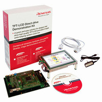
Manufacturer Part Number
YLCDRSK2378
Description
KIT DEV EVAL H8S/2378 LCD
Manufacturer
Renesas Electronics America
Series
H8®r
Datasheet
1.YR0K42378FC000BA.pdf
(1208 pages)
Specifications of YLCDRSK2378
Main Purpose
Displays, LCD Controller
Embedded
Yes, MCU, 16-Bit
Utilized Ic / Part
YLCDRSK2378
Primary Attributes
5.7" QVGA, Touch Screen
Secondary Attributes
Source Code on CD, Debugging Requires Emulator Cable E10A USB/JTAG
Lead Free Status / RoHS Status
Lead free / RoHS Compliant


1. Set up the TPU channel to be used as the output trigger channel so that TGRA and TGRB are
2. Write H'FF in P1DDR and NDERH, and set the G3CMS1, G3CMS0, G2CMS1, and G2CMS0
3. The timer counter in the TPU channel starts. When a compare match with TGRB occurs,
4. Four-phase complementary non-overlapping pulse output can be obtained subsequently by
output compare registers. Set the trigger period in TGRB and the non-overlap margin in
TGRA, and set the counter to be cleared by compare match B. Set the TGIEA bit in TIER to 1
to enable the TGIA interrupt.
bits in PCR to select compare match in the TPU channel set up in the previous step to be the
output trigger. Set the G3NOV and G2NOV bits in PMR to 1 to select non-overlapping output.
Write output data H'95 in NDRH.
outputs change from 1 to 0. When a compare match with TGRA occurs, outputs change from 0
to 1 (the change from 0 to 1 is delayed by the value set in TGRA). The TGIA interrupt
handling routine writes the next output data (H'65) in NDRH.
writing H'59, H'56, H'95... at successive TGIA interrupts.
If the DTC or DMAC is set for activation by the TGIA interrupt, pulse output can be obtained
without imposing a load on the CPU.
Section 12 Programmable Pulse Generator (PPG)
Rev.7.00 Mar. 18, 2009 page 649 of 1136
REJ09B0109-0700
Related parts for YLCDRSK2378
Image
Part Number
Description
Manufacturer
Datasheet
Request
R

Part Number:
Description:
KIT STARTER FOR M16C/29
Manufacturer:
Renesas Electronics America
Datasheet:

Part Number:
Description:
KIT STARTER FOR R8C/2D
Manufacturer:
Renesas Electronics America
Datasheet:

Part Number:
Description:
R0K33062P STARTER KIT
Manufacturer:
Renesas Electronics America
Datasheet:

Part Number:
Description:
KIT STARTER FOR R8C/23 E8A
Manufacturer:
Renesas Electronics America
Datasheet:

Part Number:
Description:
KIT STARTER FOR R8C/25
Manufacturer:
Renesas Electronics America
Datasheet:

Part Number:
Description:
KIT STARTER H8S2456 SHARPE DSPLY
Manufacturer:
Renesas Electronics America
Datasheet:

Part Number:
Description:
KIT STARTER FOR R8C38C
Manufacturer:
Renesas Electronics America
Datasheet:

Part Number:
Description:
KIT STARTER FOR R8C35C
Manufacturer:
Renesas Electronics America
Datasheet:

Part Number:
Description:
KIT STARTER FOR R8CL3AC+LCD APPS
Manufacturer:
Renesas Electronics America
Datasheet:
Part Number:
Description:
KIT STARTER FOR RX610
Manufacturer:
Renesas Electronics America
Datasheet:

Part Number:
Description:
KIT STARTER FOR R32C/118
Manufacturer:
Renesas Electronics America
Datasheet:

Part Number:
Description:
KIT DEV RSK-R8C/26-29
Manufacturer:
Renesas Electronics America
Datasheet:

Part Number:
Description:
KIT STARTER FOR SH7124
Manufacturer:
Renesas Electronics America
Datasheet:

Part Number:
Description:
KIT STARTER FOR H8SX/1622
Manufacturer:
Renesas Electronics America
Datasheet:

Part Number:
Description:
KIT DEV FOR SH7203
Manufacturer:
Renesas Electronics America
Datasheet: