YLCDRSK2378 Renesas Electronics America, YLCDRSK2378 Datasheet - Page 28
YLCDRSK2378
Manufacturer Part Number
YLCDRSK2378
Description
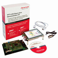
KIT DEV EVAL H8S/2378 LCD
Manufacturer
Renesas Electronics America
Series
H8®r
Datasheet
1.YR0K42378FC000BA.pdf
(1208 pages)
Specifications of YLCDRSK2378
Main Purpose
Displays, LCD Controller
Embedded
Yes, MCU, 16-Bit
Utilized Ic / Part
YLCDRSK2378
Primary Attributes
5.7" QVGA, Touch Screen
Secondary Attributes
Source Code on CD, Debugging Requires Emulator Cable E10A USB/JTAG
Lead Free Status / RoHS Status
Lead free / RoHS Compliant


6.5
6.6
6.7
Rev.7.00 Mar. 18, 2009 page xxvi of lxvi
REJ09B0109-0700
6.4.2
6.4.3
6.4.4
Basic Bus Interface ............................................................................................................ 176
6.5.1
6.5.2
6.5.3
6.5.4
6.5.5
6.5.6
DRAM Interface ................................................................................................................ 191
6.6.1
6.6.2
6.6.3
6.6.4
6.6.5
6.6.6
6.6.7
6.6.8
6.6.9
6.6.10 Byte Access Control ............................................................................................. 202
6.6.11 Burst Operation..................................................................................................... 203
6.6.12 Refresh Control..................................................................................................... 208
6.6.13 DMAC and EXDMAC Single Address Transfer Mode and DRAM Interface ..... 213
Synchronous DRAM Interface........................................................................................... 216
6.7.1
6.7.2
6.7.3
6.7.4
6.7.5
6.7.6
6.7.7
6.7.8
6.7.9
6.7.10 Bus Cycle Control in Write Cycle ........................................................................ 227
6.7.11 Byte Access Control ............................................................................................. 228
6.7.12 Burst Operation..................................................................................................... 231
6.7.13 Refresh Control..................................................................................................... 234
6.7.14 Mode Register Setting of Synchronous DRAM.................................................... 240
6.7.15 DMAC and EXDMAC Single Address Transfer Mode
Bus Specifications................................................................................................. 172
Memory Interfaces ................................................................................................ 174
Chip Select Signals ............................................................................................... 175
Data Size and Data Alignment.............................................................................. 176
Valid Strobes......................................................................................................... 178
Basic Timing......................................................................................................... 178
Wait Control ......................................................................................................... 187
Read Strobe (RD) Timing ..................................................................................... 188
Extension of Chip Select (CS) Assertion Period................................................... 189
Setting DRAM Space............................................................................................ 191
Address Multiplexing............................................................................................ 191
Data Bus................................................................................................................ 192
Pins Used for DRAM Interface............................................................................. 193
Basic Timing......................................................................................................... 194
Column Address Output Cycle Control ................................................................ 195
Row Address Output State Control....................................................................... 196
Precharge State Control ........................................................................................ 198
Wait Control ......................................................................................................... 199
Setting Continuous Synchronous DRAM Space................................................... 216
Address Multiplexing............................................................................................ 217
Data Bus................................................................................................................ 218
Pins Used for Synchronous DRAM Interface ....................................................... 218
Synchronous DRAM Clock .................................................................................. 220
Basic Timing......................................................................................................... 220
CAS Latency Control............................................................................................ 222
Row Address Output State Control....................................................................... 224
Precharge State Count........................................................................................... 225
and Synchronous DRAM Interface....................................................................... 241
Related parts for YLCDRSK2378
Image
Part Number
Description
Manufacturer
Datasheet
Request
R

Part Number:
Description:
KIT STARTER FOR M16C/29
Manufacturer:
Renesas Electronics America
Datasheet:

Part Number:
Description:
KIT STARTER FOR R8C/2D
Manufacturer:
Renesas Electronics America
Datasheet:

Part Number:
Description:
R0K33062P STARTER KIT
Manufacturer:
Renesas Electronics America
Datasheet:

Part Number:
Description:
KIT STARTER FOR R8C/23 E8A
Manufacturer:
Renesas Electronics America
Datasheet:

Part Number:
Description:
KIT STARTER FOR R8C/25
Manufacturer:
Renesas Electronics America
Datasheet:

Part Number:
Description:
KIT STARTER H8S2456 SHARPE DSPLY
Manufacturer:
Renesas Electronics America
Datasheet:

Part Number:
Description:
KIT STARTER FOR R8C38C
Manufacturer:
Renesas Electronics America
Datasheet:

Part Number:
Description:
KIT STARTER FOR R8C35C
Manufacturer:
Renesas Electronics America
Datasheet:

Part Number:
Description:
KIT STARTER FOR R8CL3AC+LCD APPS
Manufacturer:
Renesas Electronics America
Datasheet:
Part Number:
Description:
KIT STARTER FOR RX610
Manufacturer:
Renesas Electronics America
Datasheet:

Part Number:
Description:
KIT STARTER FOR R32C/118
Manufacturer:
Renesas Electronics America
Datasheet:

Part Number:
Description:
KIT DEV RSK-R8C/26-29
Manufacturer:
Renesas Electronics America
Datasheet:

Part Number:
Description:
KIT STARTER FOR SH7124
Manufacturer:
Renesas Electronics America
Datasheet:

Part Number:
Description:
KIT STARTER FOR H8SX/1622
Manufacturer:
Renesas Electronics America
Datasheet:

Part Number:
Description:
KIT DEV FOR SH7203
Manufacturer:
Renesas Electronics America
Datasheet: