YLCDRSK2378 Renesas Electronics America, YLCDRSK2378 Datasheet - Page 921
YLCDRSK2378
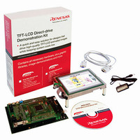
Manufacturer Part Number
YLCDRSK2378
Description
KIT DEV EVAL H8S/2378 LCD
Manufacturer
Renesas Electronics America
Series
H8®r
Datasheet
1.YR0K42378FC000BA.pdf
(1208 pages)
Specifications of YLCDRSK2378
Main Purpose
Displays, LCD Controller
Embedded
Yes, MCU, 16-Bit
Utilized Ic / Part
YLCDRSK2378
Primary Attributes
5.7" QVGA, Touch Screen
Secondary Attributes
Source Code on CD, Debugging Requires Emulator Cable E10A USB/JTAG
Lead Free Status / RoHS Status
Lead free / RoHS Compliant


Notes: 1. Prewriting (setting erase block data to all 0) is not necessary.
2. The values of x, y, z, α, β, γ, ε, η, θ, and N are shown in section 26.1.6, Flash Memory Characteristics.
3. Verify data is read in 16-bit (W) units.
4. Set only one bit in EBR1 or EBR2. More than one bit cannot be set.
5. Erasing is performed in block units. To erase a number of blocks, the individual blocks must be erased sequentially.
Increment
address
NG
NG
Figure 20.8 Erase/Erase-Verify Flowchart
Set block start address to verify address
H'FF dummy write to verify address
*5
Clear ESU bit in FLMCR1
Clear SWE bit in FLMCR1
Set SWE bit in FLMCR1
Set ESU bit in FLMCR1
Clear EV bit in FLMCR1
Clear E bit in FLMCR1
Set EV bit in FLMCR1
Last address of block?
Set E bit in FLMCR1
erasing of all erase
Verify data = all 1?
Set EBR1, EBR2
Read verify data
End of erasing
Disable WDT
Enable WDT
Wait (α) μs
Wait (η) μs
Wait (x) μs
Wait (y) μs
Wait (z) μs
Wait (β) μs
Wait (ε) μs
Wait (θ) μs
Wait (γ) μs
blocks?
End of
n = 1
Start
OK
OK
OK
*1
Section 20 Flash Memory (0.35-μm F-ZTAT Version)
*2
NG
*2
*2
*4
*2
Start of erase
*2
Halt erase
*2
*2
*2
*2
*3
Rev.7.00 Mar. 18, 2009 page 853 of 1136
Clear SWE bit in FLMCR1
Clear EV bit in FLMCR1
Erase failure
Wait (η) μs
Wait (θ) μs
n ≥ N?
OK
*2
REJ09B0109-0700
NG
*2
n ← n + 1
*2
Related parts for YLCDRSK2378
Image
Part Number
Description
Manufacturer
Datasheet
Request
R

Part Number:
Description:
KIT STARTER FOR M16C/29
Manufacturer:
Renesas Electronics America
Datasheet:

Part Number:
Description:
KIT STARTER FOR R8C/2D
Manufacturer:
Renesas Electronics America
Datasheet:

Part Number:
Description:
R0K33062P STARTER KIT
Manufacturer:
Renesas Electronics America
Datasheet:

Part Number:
Description:
KIT STARTER FOR R8C/23 E8A
Manufacturer:
Renesas Electronics America
Datasheet:

Part Number:
Description:
KIT STARTER FOR R8C/25
Manufacturer:
Renesas Electronics America
Datasheet:

Part Number:
Description:
KIT STARTER H8S2456 SHARPE DSPLY
Manufacturer:
Renesas Electronics America
Datasheet:

Part Number:
Description:
KIT STARTER FOR R8C38C
Manufacturer:
Renesas Electronics America
Datasheet:

Part Number:
Description:
KIT STARTER FOR R8C35C
Manufacturer:
Renesas Electronics America
Datasheet:

Part Number:
Description:
KIT STARTER FOR R8CL3AC+LCD APPS
Manufacturer:
Renesas Electronics America
Datasheet:
Part Number:
Description:
KIT STARTER FOR RX610
Manufacturer:
Renesas Electronics America
Datasheet:

Part Number:
Description:
KIT STARTER FOR R32C/118
Manufacturer:
Renesas Electronics America
Datasheet:

Part Number:
Description:
KIT DEV RSK-R8C/26-29
Manufacturer:
Renesas Electronics America
Datasheet:

Part Number:
Description:
KIT STARTER FOR SH7124
Manufacturer:
Renesas Electronics America
Datasheet:

Part Number:
Description:
KIT STARTER FOR H8SX/1622
Manufacturer:
Renesas Electronics America
Datasheet:

Part Number:
Description:
KIT DEV FOR SH7203
Manufacturer:
Renesas Electronics America
Datasheet: