YLCDRSK2378 Renesas Electronics America, YLCDRSK2378 Datasheet - Page 52
YLCDRSK2378
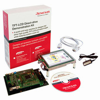
Manufacturer Part Number
YLCDRSK2378
Description
KIT DEV EVAL H8S/2378 LCD
Manufacturer
Renesas Electronics America
Series
H8®r
Datasheet
1.YR0K42378FC000BA.pdf
(1208 pages)
Specifications of YLCDRSK2378
Main Purpose
Displays, LCD Controller
Embedded
Yes, MCU, 16-Bit
Utilized Ic / Part
YLCDRSK2378
Primary Attributes
5.7" QVGA, Touch Screen
Secondary Attributes
Source Code on CD, Debugging Requires Emulator Cable E10A USB/JTAG
Lead Free Status / RoHS Status
Lead free / RoHS Compliant


Figure 8.40 External Request/Cycle Steal Mode/Block Transfer Mode
Figure 8.41 External Request/Cycle Steal Mode/Block Transfer Mode
Figure 8.42 External Request/Cycle Steal Mode/Block Transfer Mode
Figure 8.43 External Request/Cycle Steal Mode/Block Transfer Mode
Figure 8.44 External Request/Cycle Steal Mode/Block Transfer Mode
Figure 8.45 Transfer End Interrupt Logic................................................................................... 420
Figure 8.46 Example of Procedure for Restarting Transfer on Channel
Section 9 Data Transfer Controller (DTC) ........................................................ 425
Figure 9.1
Figure 9.2
Figure 9.3
Figure 9.4
Figure 9.5
Figure 9.6
Figure 9.7
Figure 9.8
Figure 9.9
Figure 9.10 DTC Operation Timing (Example in Normal Mode or Repeat Mode) ................... 444
Figure 9.11 DTC Operation Timing (Example of Block Transfer Mode,
Figure 9.12 DTC Operation Timing (Example of Chain Transfer) ............................................ 445
Figure 9.13 Chain Transfer when Counter = 0 ........................................................................... 451
Section 11 16-Bit Timer Pulse Unit (TPU) ....................................................... 545
Figure 11.1 Block Diagram of TPU............................................................................................ 548
Figure 11.2 Example of Counter Operation Setting Procedure .................................................. 583
Figure 11.3 Free-Running Counter Operation ............................................................................ 584
Figure 11.4 Periodic Counter Operation..................................................................................... 585
Figure 11.5 Example of Setting Procedure for Waveform Output by Compare Match.............. 586
Figure 11.6 Example of 0 Output/1 Output Operation ............................................................... 587
Figure 11.7 Example of Toggle Output Operation ..................................................................... 587
Figure 11.8 Example of Setting Procedure for Input Capture Operation.................................... 588
Figure 11.9 Example of Input Capture Operation ...................................................................... 589
Figure 11.10 Example of Synchronous Operation Setting Procedure .......................................... 590
Rev.7.00 Mar. 18, 2009 page l of lxvi
REJ09B0109-0700
(No Contention/Single Address Mode/Falling Edge Sensing/BGUP = 0) .............. 413
(CPU Cycles/Single Address Mode/Low Level Sensing/BGUP = 0) ..................... 414
(CPU Cycles/Dual Address Mode/Low Level Sensing/BGUP = 1)........................ 415
(CPU Cycles/Single Address Mode/Low Level Sensing/BGUP = 1) ..................... 416
(Contention with Another Channel/Dual Address Mode/Low Level Sensing) ....... 417
in which Transfer End Interrupt Occurred .............................................................. 421
Block Diagram of DTC ........................................................................................... 426
Block Diagram of DTC Activation Source Control ................................................ 433
Correspondence between DTC Vector Address and Register Information ............. 434
Correspondence between DTC Vector Address and Register Information ............. 434
Flowchart of DTC Operation .................................................................................. 438
Memory Mapping in Normal Mode ........................................................................ 440
Memory Mapping in Repeat Mode ......................................................................... 441
Memory Mapping in Block Transfer Mode ............................................................ 442
Operation of Chain Transfer.................................................................................... 443
with Block Size of 2)............................................................................................... 445
Related parts for YLCDRSK2378
Image
Part Number
Description
Manufacturer
Datasheet
Request
R

Part Number:
Description:
KIT STARTER FOR M16C/29
Manufacturer:
Renesas Electronics America
Datasheet:

Part Number:
Description:
KIT STARTER FOR R8C/2D
Manufacturer:
Renesas Electronics America
Datasheet:

Part Number:
Description:
R0K33062P STARTER KIT
Manufacturer:
Renesas Electronics America
Datasheet:

Part Number:
Description:
KIT STARTER FOR R8C/23 E8A
Manufacturer:
Renesas Electronics America
Datasheet:

Part Number:
Description:
KIT STARTER FOR R8C/25
Manufacturer:
Renesas Electronics America
Datasheet:

Part Number:
Description:
KIT STARTER H8S2456 SHARPE DSPLY
Manufacturer:
Renesas Electronics America
Datasheet:

Part Number:
Description:
KIT STARTER FOR R8C38C
Manufacturer:
Renesas Electronics America
Datasheet:

Part Number:
Description:
KIT STARTER FOR R8C35C
Manufacturer:
Renesas Electronics America
Datasheet:

Part Number:
Description:
KIT STARTER FOR R8CL3AC+LCD APPS
Manufacturer:
Renesas Electronics America
Datasheet:
Part Number:
Description:
KIT STARTER FOR RX610
Manufacturer:
Renesas Electronics America
Datasheet:

Part Number:
Description:
KIT STARTER FOR R32C/118
Manufacturer:
Renesas Electronics America
Datasheet:

Part Number:
Description:
KIT DEV RSK-R8C/26-29
Manufacturer:
Renesas Electronics America
Datasheet:

Part Number:
Description:
KIT STARTER FOR SH7124
Manufacturer:
Renesas Electronics America
Datasheet:

Part Number:
Description:
KIT STARTER FOR H8SX/1622
Manufacturer:
Renesas Electronics America
Datasheet:

Part Number:
Description:
KIT DEV FOR SH7203
Manufacturer:
Renesas Electronics America
Datasheet: