YLCDRSK2378 Renesas Electronics America, YLCDRSK2378 Datasheet - Page 267
YLCDRSK2378
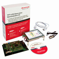
Manufacturer Part Number
YLCDRSK2378
Description
KIT DEV EVAL H8S/2378 LCD
Manufacturer
Renesas Electronics America
Series
H8®r
Datasheet
1.YR0K42378FC000BA.pdf
(1208 pages)
Specifications of YLCDRSK2378
Main Purpose
Displays, LCD Controller
Embedded
Yes, MCU, 16-Bit
Utilized Ic / Part
YLCDRSK2378
Primary Attributes
5.7" QVGA, Touch Screen
Secondary Attributes
Source Code on CD, Debugging Requires Emulator Cable E10A USB/JTAG
Lead Free Status / RoHS Status
Lead free / RoHS Compliant


Section 6 Bus Controller (BSC)
6.6.9
Wait Control
There are two ways of inserting wait states in a DRAM access cycle: program wait insertion and
pin wait insertion using the WAIT pin.
Wait states are inserted to extend the CAS assertion period in a read access to DRAM space, and
to extend the write data setup time relative to the falling edge of CAS in a write access.
Program Wait Insertion: When the bit in ASTCR corresponding to an area designated as DRAM
space is set to 1, from 0 to 7 wait states can be inserted automatically between the T
state and T
c1
c2
state, according to the settings in WTCR.
Pin Wait Insertion: When the WAITE bit in BCR is set to 1 and the ASTCR bit is set to 1, wait
input by means of the WAIT pin is enabled. When DRAM space is accessed in this state, a
) is first inserted. If the WAIT pin is low at the falling edge of φ in the last T
program wait (T
or
w
c1
state is inserted. If the WAIT pin is held low, T
T
state, another T
states are inserted until it
w
w
w
goes high.
Figures 6.26 and 6.27 show examples of wait cycle insertion timing in the case of 2-state and 3-
state column address output cycles.
Rev.7.00 Mar. 18, 2009 page 199 of 1136
REJ09B0109-0700
Related parts for YLCDRSK2378
Image
Part Number
Description
Manufacturer
Datasheet
Request
R

Part Number:
Description:
KIT STARTER FOR M16C/29
Manufacturer:
Renesas Electronics America
Datasheet:

Part Number:
Description:
KIT STARTER FOR R8C/2D
Manufacturer:
Renesas Electronics America
Datasheet:

Part Number:
Description:
R0K33062P STARTER KIT
Manufacturer:
Renesas Electronics America
Datasheet:

Part Number:
Description:
KIT STARTER FOR R8C/23 E8A
Manufacturer:
Renesas Electronics America
Datasheet:

Part Number:
Description:
KIT STARTER FOR R8C/25
Manufacturer:
Renesas Electronics America
Datasheet:

Part Number:
Description:
KIT STARTER H8S2456 SHARPE DSPLY
Manufacturer:
Renesas Electronics America
Datasheet:

Part Number:
Description:
KIT STARTER FOR R8C38C
Manufacturer:
Renesas Electronics America
Datasheet:

Part Number:
Description:
KIT STARTER FOR R8C35C
Manufacturer:
Renesas Electronics America
Datasheet:

Part Number:
Description:
KIT STARTER FOR R8CL3AC+LCD APPS
Manufacturer:
Renesas Electronics America
Datasheet:
Part Number:
Description:
KIT STARTER FOR RX610
Manufacturer:
Renesas Electronics America
Datasheet:

Part Number:
Description:
KIT STARTER FOR R32C/118
Manufacturer:
Renesas Electronics America
Datasheet:

Part Number:
Description:
KIT DEV RSK-R8C/26-29
Manufacturer:
Renesas Electronics America
Datasheet:

Part Number:
Description:
KIT STARTER FOR SH7124
Manufacturer:
Renesas Electronics America
Datasheet:

Part Number:
Description:
KIT STARTER FOR H8SX/1622
Manufacturer:
Renesas Electronics America
Datasheet:

Part Number:
Description:
KIT DEV FOR SH7203
Manufacturer:
Renesas Electronics America
Datasheet: