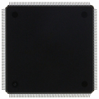
MCF5307AI90B Freescale Semiconductor, MCF5307AI90B Datasheet - Page 101

MCF5307AI90B
Manufacturer Part Number
MCF5307AI90B
Description
IC MPU 32BIT COLDF 90MHZ 208FQFP
Manufacturer
Freescale Semiconductor
Series
MCF530xr
Datasheets
1.MCF5307AI66B.pdf
(484 pages)
2.MCF5307AI66B.pdf
(16 pages)
3.MCF5307AI66B.pdf
(2 pages)
Specifications of MCF5307AI90B
Core Processor
Coldfire V3
Core Size
32-Bit
Speed
90MHz
Connectivity
EBI/EMI, I²C, UART/USART
Peripherals
DMA, POR, WDT
Number Of I /o
16
Program Memory Type
ROMless
Ram Size
4K x 8
Voltage - Supply (vcc/vdd)
3 V ~ 3.6 V
Oscillator Type
External
Operating Temperature
0°C ~ 70°C
Package / Case
208-FQFP
Maximum Clock Frequency
90 MHz
Maximum Operating Temperature
+ 105 C
Mounting Style
SMD/SMT
Minimum Operating Temperature
0 C
Family Name
MCF5xxx
Device Core
ColdFire
Device Core Size
32b
Frequency (max)
90MHz
Instruction Set Architecture
RISC
Supply Voltage 1 (typ)
3.3V
Operating Temp Range
0C to 70C
Operating Temperature Classification
Commercial
Mounting
Surface Mount
Pin Count
208
Package Type
FQFP
Program Memory Size
8KB
Cpu Speed
90MHz
Embedded Interface Type
I2C, UART
Digital Ic Case Style
FQFP
No. Of Pins
208
Supply Voltage Range
3V To 3.6V
Rohs Compliant
Yes
Lead Free Status / RoHS Status
Lead free / RoHS Compliant
Eeprom Size
-
Program Memory Size
-
Data Converters
-
Lead Free Status / Rohs Status
Lead free / RoHS Compliant
Available stocks
Company
Part Number
Manufacturer
Quantity
Price
Company:
Part Number:
MCF5307AI90B
Manufacturer:
FREESCAL
Quantity:
153
Company:
Part Number:
MCF5307AI90B
Manufacturer:
Freescale Semiconductor
Quantity:
10 000
Part Number:
MCF5307AI90B
Manufacturer:
FREESCALE
Quantity:
20 000
- Current page: 101 of 484
- Download datasheet (6Mb)
Accesses are attempted in the following order:
4.4 SRAM Programming Model
The SRAM programming model consists of RAMBAR.
4.4.1 SRAM Base Address Register (RAMBAR)
The SRAM modules are configured through the RAMBAR, shown in Figure 4-1.
Address
RAMBAR fields are described in detail in Table 4-1.
31–15 BA
14–9
8
7–6
Bits
Reset
Field
R/W
1. SRAM
2. Cache (if space is defined as cacheable)
3. External access
• RAMBAR holds the base address of the SRAM. The MOVEC instruction provides
• RAMBAR can be read or written from the debug module in a similar manner.
• All undefined RAMBAR bits are reserved. These bits are ignored during writes to
• The valid bit, RAMBAR[V], is cleared at reset, disabling the SRAM module. All
write-only access to this register from the processor.
the RAMBAR and return zeros when read from the debug module.
other bits are unaffected.
—
WP
—
31
Name
Base address. Defines the SRAM module’s word-aligned base address. The SRAM module
occupies a 4-Kbyte space defined by the contents of BA. SRAM may reside on any 32-Kbyte
boundary in the 4-Gbyte address space.
Reserved, should be cleared.
Write protect. Controls read/write properties of the SRAM.
0 Allows read and write accesses to the SRAM module
1 Allows only read accesses to the SRAM module. Any attempted write reference generates an
Reserved, should be cleared.
access error exception to the ColdFire processor core.
Figure 4-1. SRAM Base Address Register (RAMBAR)
BA
Freescale Semiconductor, Inc.
Table 4-1. RAMBAR Field Description
For More Information On This Product,
Chapter 4. Local Memory
Go to: www.freescale.com
15
W for CPU; R/W for debug
14
CPU space + 0xC04
—
—
Description
9
WP
8
7
—
SRAM Programming Model
6
C/I SC SD UC UD
5
4
3
2
1
4-3
V
0
0
Related parts for MCF5307AI90B
Image
Part Number
Description
Manufacturer
Datasheet
Request
R
Part Number:
Description:
Manufacturer:
Freescale Semiconductor, Inc
Datasheet:
Part Number:
Description:
Mcf5307 Coldfire Integrated Microprocessor User
Manufacturer:
Freescale Semiconductor, Inc
Datasheet:
Part Number:
Description:
Manufacturer:
Freescale Semiconductor, Inc
Datasheet:
Part Number:
Description:
Manufacturer:
Freescale Semiconductor, Inc
Datasheet:
Part Number:
Description:
Manufacturer:
Freescale Semiconductor, Inc
Datasheet:
Part Number:
Description:
Manufacturer:
Freescale Semiconductor, Inc
Datasheet:
Part Number:
Description:
Manufacturer:
Freescale Semiconductor, Inc
Datasheet:
Part Number:
Description:
Manufacturer:
Freescale Semiconductor, Inc
Datasheet:
Part Number:
Description:
Manufacturer:
Freescale Semiconductor, Inc
Datasheet:
Part Number:
Description:
Manufacturer:
Freescale Semiconductor, Inc
Datasheet:
Part Number:
Description:
Manufacturer:
Freescale Semiconductor, Inc
Datasheet:
Part Number:
Description:
Manufacturer:
Freescale Semiconductor, Inc
Datasheet:
Part Number:
Description:
Manufacturer:
Freescale Semiconductor, Inc
Datasheet:
Part Number:
Description:
Manufacturer:
Freescale Semiconductor, Inc
Datasheet:
Part Number:
Description:
Manufacturer:
Freescale Semiconductor, Inc
Datasheet:


