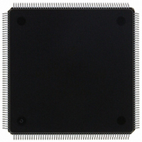
MCF5307AI90B Freescale Semiconductor, MCF5307AI90B Datasheet - Page 369

MCF5307AI90B
Manufacturer Part Number
MCF5307AI90B
Description
IC MPU 32BIT COLDF 90MHZ 208FQFP
Manufacturer
Freescale Semiconductor
Series
MCF530xr
Datasheets
1.MCF5307AI66B.pdf
(484 pages)
2.MCF5307AI66B.pdf
(16 pages)
3.MCF5307AI66B.pdf
(2 pages)
Specifications of MCF5307AI90B
Core Processor
Coldfire V3
Core Size
32-Bit
Speed
90MHz
Connectivity
EBI/EMI, I²C, UART/USART
Peripherals
DMA, POR, WDT
Number Of I /o
16
Program Memory Type
ROMless
Ram Size
4K x 8
Voltage - Supply (vcc/vdd)
3 V ~ 3.6 V
Oscillator Type
External
Operating Temperature
0°C ~ 70°C
Package / Case
208-FQFP
Maximum Clock Frequency
90 MHz
Maximum Operating Temperature
+ 105 C
Mounting Style
SMD/SMT
Minimum Operating Temperature
0 C
Family Name
MCF5xxx
Device Core
ColdFire
Device Core Size
32b
Frequency (max)
90MHz
Instruction Set Architecture
RISC
Supply Voltage 1 (typ)
3.3V
Operating Temp Range
0C to 70C
Operating Temperature Classification
Commercial
Mounting
Surface Mount
Pin Count
208
Package Type
FQFP
Program Memory Size
8KB
Cpu Speed
90MHz
Embedded Interface Type
I2C, UART
Digital Ic Case Style
FQFP
No. Of Pins
208
Supply Voltage Range
3V To 3.6V
Rohs Compliant
Yes
Lead Free Status / RoHS Status
Lead free / RoHS Compliant
Eeprom Size
-
Program Memory Size
-
Data Converters
-
Lead Free Status / Rohs Status
Lead free / RoHS Compliant
Available stocks
Company
Part Number
Manufacturer
Quantity
Price
Company:
Part Number:
MCF5307AI90B
Manufacturer:
FREESCAL
Quantity:
153
Company:
Part Number:
MCF5307AI90B
Manufacturer:
Freescale Semiconductor
Quantity:
10 000
Part Number:
MCF5307AI90B
Manufacturer:
FREESCALE
Quantity:
20 000
- Current page: 369 of 484
- Download datasheet (6Mb)
1
2
Table 17-2 lists signals in alphabetical order by abbreviated name.
Parallel port
Serial clock line
Serial data line
Motorola test mode
Motorola test mode
High impedance
Processor clock out
Processor status
Debug data
Test clock
Test reset/
Development serial
clock
Test mode select/
Breakpoint
Test data input/
Development serial
input
Test data output/
Development serial
output
If there is no arbiter, BG should be tied low; otherwise, it should be negated.
These data pins are sampled at reset for configuration.
AA_CONFIG
ADDR_CONFIG
AS
A[31:0]
Abbreviation
Signal Name
Auto-acknowledge configuration
Address configuration
Address strobe
Address
Table 17-1. MCF5307 Signal Index (Continued)
Table 17-2. MCF507 Alphabetical Signal Index
PP[15:0]
SCL
SDA
MTMOD0
MTMOD[3:1]
HIZ
PSTCLK
PST[3:0]
DDATA[3:0]
TCK
TRST/DSCLK
TMS/BKPT
TDI/DSI
TDO/DSO
Abbreviation
Freescale Semiconductor, Inc.
Section 17.14, “Debug Module/JTAG Signals”
For More Information On This Product,
Section 17.13, “Debug and Test Signals”
Section 17.12, “I
Chapter 17. Signal Descriptions
Signal Name
Go to: www.freescale.com
Interfaces with I/O; multiplexed with
bus address and attribute signals.
Clock signal for I
Serial data port for I
Puts processor in functional or
emulator mode
Reserved
Assertion three-states all outputs
Output clock used for PSTDDATA
Displays captured processor data .
Displays captured processor data
and breakpoint status.
Clock signal for IEEE 1149.1 JTAG
Asynchronous reset for JTAG;
debug module clock input
TMS (JTAG)/hardware breakpoint
(debug)
Multiplexed serial input for the JTAG
or background debug module
Multiplexed serial output for the
JTAG or background debug module
2
C Module Signals”
Function
2
C operation
2
C operation
Clock/reset
Clock/reset
Bus
Bus
Function
I/O
I/O
I/O
I/O
O
O
O
O
I
I
I
I
I
I
I
Driven
Driven
Driven
Reset
Open
Open
Input
drain
drain
—
—
—
—
—
—
—
—
User cfg 17-20
I/O
I/O
I/O
Pull-Up Page
I
I
Down
Low
Up
Up
Up
Up
Up
Up
Overview
17-14
17-14
Page
17-9
17-7
17-19
17-19
17-19
17-19
17-20
17-20
17-20
17-20
17-20
17-20
17-21
17-23
17-21
17-22
17-22
17-22
17-5
Related parts for MCF5307AI90B
Image
Part Number
Description
Manufacturer
Datasheet
Request
R
Part Number:
Description:
Manufacturer:
Freescale Semiconductor, Inc
Datasheet:
Part Number:
Description:
Mcf5307 Coldfire Integrated Microprocessor User
Manufacturer:
Freescale Semiconductor, Inc
Datasheet:
Part Number:
Description:
Manufacturer:
Freescale Semiconductor, Inc
Datasheet:
Part Number:
Description:
Manufacturer:
Freescale Semiconductor, Inc
Datasheet:
Part Number:
Description:
Manufacturer:
Freescale Semiconductor, Inc
Datasheet:
Part Number:
Description:
Manufacturer:
Freescale Semiconductor, Inc
Datasheet:
Part Number:
Description:
Manufacturer:
Freescale Semiconductor, Inc
Datasheet:
Part Number:
Description:
Manufacturer:
Freescale Semiconductor, Inc
Datasheet:
Part Number:
Description:
Manufacturer:
Freescale Semiconductor, Inc
Datasheet:
Part Number:
Description:
Manufacturer:
Freescale Semiconductor, Inc
Datasheet:
Part Number:
Description:
Manufacturer:
Freescale Semiconductor, Inc
Datasheet:
Part Number:
Description:
Manufacturer:
Freescale Semiconductor, Inc
Datasheet:
Part Number:
Description:
Manufacturer:
Freescale Semiconductor, Inc
Datasheet:
Part Number:
Description:
Manufacturer:
Freescale Semiconductor, Inc
Datasheet:
Part Number:
Description:
Manufacturer:
Freescale Semiconductor, Inc
Datasheet:


