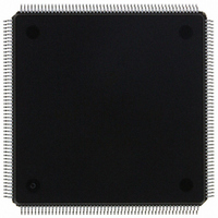
MCF5307AI90B Freescale Semiconductor, MCF5307AI90B Datasheet - Page 232

MCF5307AI90B
Manufacturer Part Number
MCF5307AI90B
Description
IC MPU 32BIT COLDF 90MHZ 208FQFP
Manufacturer
Freescale Semiconductor
Series
MCF530xr
Datasheets
1.MCF5307AI66B.pdf
(484 pages)
2.MCF5307AI66B.pdf
(16 pages)
3.MCF5307AI66B.pdf
(2 pages)
Specifications of MCF5307AI90B
Core Processor
Coldfire V3
Core Size
32-Bit
Speed
90MHz
Connectivity
EBI/EMI, I²C, UART/USART
Peripherals
DMA, POR, WDT
Number Of I /o
16
Program Memory Type
ROMless
Ram Size
4K x 8
Voltage - Supply (vcc/vdd)
3 V ~ 3.6 V
Oscillator Type
External
Operating Temperature
0°C ~ 70°C
Package / Case
208-FQFP
Maximum Clock Frequency
90 MHz
Maximum Operating Temperature
+ 105 C
Mounting Style
SMD/SMT
Minimum Operating Temperature
0 C
Family Name
MCF5xxx
Device Core
ColdFire
Device Core Size
32b
Frequency (max)
90MHz
Instruction Set Architecture
RISC
Supply Voltage 1 (typ)
3.3V
Operating Temp Range
0C to 70C
Operating Temperature Classification
Commercial
Mounting
Surface Mount
Pin Count
208
Package Type
FQFP
Program Memory Size
8KB
Cpu Speed
90MHz
Embedded Interface Type
I2C, UART
Digital Ic Case Style
FQFP
No. Of Pins
208
Supply Voltage Range
3V To 3.6V
Rohs Compliant
Yes
Lead Free Status / RoHS Status
Lead free / RoHS Compliant
Eeprom Size
-
Program Memory Size
-
Data Converters
-
Lead Free Status / Rohs Status
Lead free / RoHS Compliant
Available stocks
Company
Part Number
Manufacturer
Quantity
Price
Company:
Part Number:
MCF5307AI90B
Manufacturer:
FREESCAL
Quantity:
153
Company:
Part Number:
MCF5307AI90B
Manufacturer:
Freescale Semiconductor
Quantity:
10 000
Part Number:
MCF5307AI90B
Manufacturer:
FREESCALE
Quantity:
20 000
- Current page: 232 of 484
- Download datasheet (6Mb)
Chip-Select Registers
10.4.1.3 Chip-Select Control Registers (CSCR0–CSCR7)
Each chip-select control register, Figure 10-4, controls the auto acknowledge, external
master support, port size, burst capability, and activation of each chip select. Note that to
support the global chip select, CS0, the CSCR0 reset values differ from the other CSCRs.
CS0 allows address decoding for boot ROM before system initialization.
Table 10-9 describes CSCRn fields.
Reset: Other CSCRs
15–14
13–10
10-8
Bits
7–6
9
8
5
4
Reset: CSCR0
Name
BSTR Burst read enable. Specifies whether burst reads are used for memory associated with each CSn.
BEM
WS
AA
PS
—
—
Address
Figure 10-4. Chip-Select Control Registers (CSCR0–CSCR7)
Field
R/W
Reserved, should be cleared.
Wait states. The number of wait states inserted before an internal transfer acknowledge is generated
(WS = 0 inserts zero wait states, WS = 0xF inserts 15 wait states). If AA = 0, TA must be asserted by
the external system regardless of the number of wait states generated. In that case, the external
transfer acknowledge ends the cycle. An external TA supersedes the generation of an internal TA.
Reserved, should be cleared.
Auto-acknowledge enable. Determines the assertion of the internal transfer acknowledge for
accesses specified by the chip-select address.
0 No internal TA is asserted. Cycle is terminated externally.
1 Internal TA is asserted as specified by WS. Note that if AA = 1 for a corresponding CSn and the
Port size. Specifies the width of the data associated with each chip select. It determines where data
is driven during write cycles and where data is sampled during read cycles. See Section 10.3.1.1,
“8-, 16-, and 32-Bit Port Sizing.”
00 32-bit port size. Valid data sampled and driven on D[31:0]
01 8-bit port size. Valid data sampled and driven on D[31:24]
1x 16-bit port size. Valid data sampled and driven on D[31:16]
Byte enable mode. Specifies the byte enable operation. Certain SRAMs have byte enables that must
be asserted during reads as well as writes. BEM can be set in the relevant CSCR to provide the
appropriate mode of byte enable in support of these SRAMs.
0 Neither BE nor BWE is asserted for read. BWE is generated for data write only.
1 BE is asserted for read; BWE is asserted for write.
0 Data exceeding the specified port size is broken into individual, port-sized non-burst reads. For
1 Enables data burst reads larger than the specified port size, including longword reads from 8- and
external system asserts an external TA before the wait-state countdown asserts the internal TA, the
cycle is terminated. Burst cycles increment the address bus between each internal termination.
example, a longword read from an 8-bit port is broken into four 8-bit reads.
16-bit ports, word reads from 8-bit ports, and line reads from 8-, 16-, and 32-bit ports.
15
—
—
14
Freescale Semiconductor, Inc.
Table 10-9. CSCRn Field Descriptions
For More Information On This Product,
0x0BA (CSCR4); 0x0C6 (CSCR5); 0x0D2 (CSCR6); 0x0DE (CSCR7)
13
0x08A (CSCR0); 0x096 (CSCR1); 0x0A2 (CSCR2); 0x0AE (CSCR3);
11_11
WS
Go to: www.freescale.com
MCF5307 User’s Manual
10
—
—
9
Description
AA PS1 PS0 BEM BSTR BSTW
D7
Unitialized
8
R/W
D6
7
D5
6
—
5
4
3
—
2
—
0
Related parts for MCF5307AI90B
Image
Part Number
Description
Manufacturer
Datasheet
Request
R
Part Number:
Description:
Manufacturer:
Freescale Semiconductor, Inc
Datasheet:
Part Number:
Description:
Mcf5307 Coldfire Integrated Microprocessor User
Manufacturer:
Freescale Semiconductor, Inc
Datasheet:
Part Number:
Description:
Manufacturer:
Freescale Semiconductor, Inc
Datasheet:
Part Number:
Description:
Manufacturer:
Freescale Semiconductor, Inc
Datasheet:
Part Number:
Description:
Manufacturer:
Freescale Semiconductor, Inc
Datasheet:
Part Number:
Description:
Manufacturer:
Freescale Semiconductor, Inc
Datasheet:
Part Number:
Description:
Manufacturer:
Freescale Semiconductor, Inc
Datasheet:
Part Number:
Description:
Manufacturer:
Freescale Semiconductor, Inc
Datasheet:
Part Number:
Description:
Manufacturer:
Freescale Semiconductor, Inc
Datasheet:
Part Number:
Description:
Manufacturer:
Freescale Semiconductor, Inc
Datasheet:
Part Number:
Description:
Manufacturer:
Freescale Semiconductor, Inc
Datasheet:
Part Number:
Description:
Manufacturer:
Freescale Semiconductor, Inc
Datasheet:
Part Number:
Description:
Manufacturer:
Freescale Semiconductor, Inc
Datasheet:
Part Number:
Description:
Manufacturer:
Freescale Semiconductor, Inc
Datasheet:
Part Number:
Description:
Manufacturer:
Freescale Semiconductor, Inc
Datasheet:


