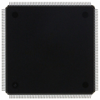
MCF5307AI90B Freescale Semiconductor, MCF5307AI90B Datasheet - Page 149

MCF5307AI90B
Manufacturer Part Number
MCF5307AI90B
Description
IC MPU 32BIT COLDF 90MHZ 208FQFP
Manufacturer
Freescale Semiconductor
Series
MCF530xr
Datasheets
1.MCF5307AI66B.pdf
(484 pages)
2.MCF5307AI66B.pdf
(16 pages)
3.MCF5307AI66B.pdf
(2 pages)
Specifications of MCF5307AI90B
Core Processor
Coldfire V3
Core Size
32-Bit
Speed
90MHz
Connectivity
EBI/EMI, I²C, UART/USART
Peripherals
DMA, POR, WDT
Number Of I /o
16
Program Memory Type
ROMless
Ram Size
4K x 8
Voltage - Supply (vcc/vdd)
3 V ~ 3.6 V
Oscillator Type
External
Operating Temperature
0°C ~ 70°C
Package / Case
208-FQFP
Maximum Clock Frequency
90 MHz
Maximum Operating Temperature
+ 105 C
Mounting Style
SMD/SMT
Minimum Operating Temperature
0 C
Family Name
MCF5xxx
Device Core
ColdFire
Device Core Size
32b
Frequency (max)
90MHz
Instruction Set Architecture
RISC
Supply Voltage 1 (typ)
3.3V
Operating Temp Range
0C to 70C
Operating Temperature Classification
Commercial
Mounting
Surface Mount
Pin Count
208
Package Type
FQFP
Program Memory Size
8KB
Cpu Speed
90MHz
Embedded Interface Type
I2C, UART
Digital Ic Case Style
FQFP
No. Of Pins
208
Supply Voltage Range
3V To 3.6V
Rohs Compliant
Yes
Lead Free Status / RoHS Status
Lead free / RoHS Compliant
Eeprom Size
-
Program Memory Size
-
Data Converters
-
Lead Free Status / Rohs Status
Lead free / RoHS Compliant
Available stocks
Company
Part Number
Manufacturer
Quantity
Price
Company:
Part Number:
MCF5307AI90B
Manufacturer:
FREESCAL
Quantity:
153
Company:
Part Number:
MCF5307AI90B
Manufacturer:
Freescale Semiconductor
Quantity:
10 000
Part Number:
MCF5307AI90B
Manufacturer:
FREESCALE
Quantity:
20 000
- Current page: 149 of 484
- Download datasheet (6Mb)
Table 5-18 describes BDM fields.
5.5.3.1.1 Extension Words as Required
Some commands require extension words for addresses and/or immediate data. Addresses
require two extension words because only absolute long addressing is permitted. Longword
accesses are forcibly longword-aligned and word accesses are forcibly word-aligned.
Immediate data can be 1 or 2 words long. Byte and word data each requires a single
extension word and longword data requires two extension words.
Operands and addresses are transferred most-significant word first. In the following
descriptions of the BDM command set, the optional set of extension words is defined as
address, data, or operand data.
5.5.3.2 Command Sequence Diagrams
The command sequence diagram in Figure 5-17 shows serial bus traffic for commands.
Each bubble represents a 17-bit bus transfer. The top half of each bubble indicates the data
the development system sends to the debug module; the bottom half indicates the debug
module’s response to the previous development system commands. Command and result
transactions overlap to minimize latency.
15–10 Operation Specifies the command. These values are listed in Table 5-17.
9
8
7–6
5–4
3
2–0
15
Bit
0
R/W
Operand
Size
00
A/D
Register
Name
Operation
Reserved
Direction of operand transfer.
0 Data is written to the CPU or to memory from the development system.
1 The transfer is from the CPU to the development system.
Operand data size for sized operations. Addresses are expressed as 32-bit absolute values.
Note that a command performing a byte-sized memory read leaves the upper 8 bits of the
response data undefined. Referenced data is returned in the lower 8 bits of the response.
00 Byte
01 Word
10 Longword
11 Reserved
Reserved
Address/data. Determines whether the register field specifies a data or address register.
0 Indicates a data register.
1 Indicates an address register.
Contains the register number in commands that operate on processor registers.
Operand Size
Freescale Semiconductor, Inc.
Figure 5-16. BDM Command Format
For More Information On This Product,
Table 5-18. BDM Field Descriptions
10
Bit Values
8 bits
16 bits
32 bits
—
Chapter 5. Debug Support
Go to: www.freescale.com
0
9
Extension Word(s)
R/W
8
7
Op Size
Description
6
0
5
Background Debug Mode (BDM)
0
4
A/D
3
2
Register
5-21
0
Related parts for MCF5307AI90B
Image
Part Number
Description
Manufacturer
Datasheet
Request
R
Part Number:
Description:
Manufacturer:
Freescale Semiconductor, Inc
Datasheet:
Part Number:
Description:
Mcf5307 Coldfire Integrated Microprocessor User
Manufacturer:
Freescale Semiconductor, Inc
Datasheet:
Part Number:
Description:
Manufacturer:
Freescale Semiconductor, Inc
Datasheet:
Part Number:
Description:
Manufacturer:
Freescale Semiconductor, Inc
Datasheet:
Part Number:
Description:
Manufacturer:
Freescale Semiconductor, Inc
Datasheet:
Part Number:
Description:
Manufacturer:
Freescale Semiconductor, Inc
Datasheet:
Part Number:
Description:
Manufacturer:
Freescale Semiconductor, Inc
Datasheet:
Part Number:
Description:
Manufacturer:
Freescale Semiconductor, Inc
Datasheet:
Part Number:
Description:
Manufacturer:
Freescale Semiconductor, Inc
Datasheet:
Part Number:
Description:
Manufacturer:
Freescale Semiconductor, Inc
Datasheet:
Part Number:
Description:
Manufacturer:
Freescale Semiconductor, Inc
Datasheet:
Part Number:
Description:
Manufacturer:
Freescale Semiconductor, Inc
Datasheet:
Part Number:
Description:
Manufacturer:
Freescale Semiconductor, Inc
Datasheet:
Part Number:
Description:
Manufacturer:
Freescale Semiconductor, Inc
Datasheet:
Part Number:
Description:
Manufacturer:
Freescale Semiconductor, Inc
Datasheet:


