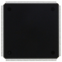
MCF5307AI90B Freescale Semiconductor, MCF5307AI90B Datasheet - Page 345

MCF5307AI90B
Manufacturer Part Number
MCF5307AI90B
Description
IC MPU 32BIT COLDF 90MHZ 208FQFP
Manufacturer
Freescale Semiconductor
Series
MCF530xr
Datasheets
1.MCF5307AI66B.pdf
(484 pages)
2.MCF5307AI66B.pdf
(16 pages)
3.MCF5307AI66B.pdf
(2 pages)
Specifications of MCF5307AI90B
Core Processor
Coldfire V3
Core Size
32-Bit
Speed
90MHz
Connectivity
EBI/EMI, I²C, UART/USART
Peripherals
DMA, POR, WDT
Number Of I /o
16
Program Memory Type
ROMless
Ram Size
4K x 8
Voltage - Supply (vcc/vdd)
3 V ~ 3.6 V
Oscillator Type
External
Operating Temperature
0°C ~ 70°C
Package / Case
208-FQFP
Maximum Clock Frequency
90 MHz
Maximum Operating Temperature
+ 105 C
Mounting Style
SMD/SMT
Minimum Operating Temperature
0 C
Family Name
MCF5xxx
Device Core
ColdFire
Device Core Size
32b
Frequency (max)
90MHz
Instruction Set Architecture
RISC
Supply Voltage 1 (typ)
3.3V
Operating Temp Range
0C to 70C
Operating Temperature Classification
Commercial
Mounting
Surface Mount
Pin Count
208
Package Type
FQFP
Program Memory Size
8KB
Cpu Speed
90MHz
Embedded Interface Type
I2C, UART
Digital Ic Case Style
FQFP
No. Of Pins
208
Supply Voltage Range
3V To 3.6V
Rohs Compliant
Yes
Lead Free Status / RoHS Status
Lead free / RoHS Compliant
Eeprom Size
-
Program Memory Size
-
Data Converters
-
Lead Free Status / Rohs Status
Lead free / RoHS Compliant
Available stocks
Company
Part Number
Manufacturer
Quantity
Price
Company:
Part Number:
MCF5307AI90B
Manufacturer:
FREESCAL
Quantity:
153
Company:
Part Number:
MCF5307AI90B
Manufacturer:
Freescale Semiconductor
Quantity:
10 000
Part Number:
MCF5307AI90B
Manufacturer:
FREESCALE
Quantity:
20 000
- Current page: 345 of 484
- Download datasheet (6Mb)
PAR[n] = 0 PP15
PAR[n] = 1 A31
Chapter 15
Parallel Port (General-Purpose I/O)
This chapter describes the operation and programming model of the parallel port pin
assignment, direction-control, and data registers. It includes a code example for setting up
the parallel port.
15.1 Parallel Port Operation
The MCF5307 parallel port module has 16 signals, which are programmed as follows:
The operations of the PAR, PADDR, and PADAT are described in the following sections.
15.1.1 Pin Assignment Register (PAR)
The pin assignment register (PAR), which is part of the system integration module (SIM),
defines how each PAR bit determines each pin function, as shown in Figure 15-1.
If PP[9:8]/A[25:24] are unavailable because A[25:0] are needed for external addressing,
PP[15:10]/A[31:26] can be configured as general-purpose I/O. Table 15-1 summarizes
MCF5307 parallel port pins, described in detail in Chapter 17, “Signal Descriptions.”
Address
• The pin assignment register (PAR) selects the function of the 16 multiplexed pins.
• Port A data direction register (PADDR) determines whether pins configured as
• The Port A data register (PADAT) shows the status of the parallel port signals.
Reset Determined by driving D4/ADDR_CONFIG with a 1 or 0 when RSTI negates. The system is configured as
Field PAR15 PAR14 PAR13 PAR12 PAR11 PAR10 PAR9 PAR8 PAR7 PAR6
R/W
parallel port signals are inputs or outputs.
PP[15:0] if D4 is low; otherwise alternate pin functions selected by PAR[n] = 1 are used.
15
Figure 15-1. Parallel Port Pin Assignment Register (PAR)
PP14
A30
14
PP13
A29
13
Chapter 15. Parallel Port (General-Purpose I/O)
Freescale Semiconductor, Inc.
PP12
For More Information On This Product,
A28
12
PP11
A27
11
Go to: www.freescale.com
PP10 PP9
A26
10
Address MBAR + 0x004
A25
9
PP8
A24
8
R/W
PP7
TIP DREQ0 DREQ1 TM2
7
PP6
6
PAR5 PAR4 PAR3
PP5
5
PP4
4
TM1
PP3
3
PAR2 PAR1 PAR0
TM0
PP2
2
PP1 PP0
TT1
1
15-1
TT0
0
Related parts for MCF5307AI90B
Image
Part Number
Description
Manufacturer
Datasheet
Request
R
Part Number:
Description:
Manufacturer:
Freescale Semiconductor, Inc
Datasheet:
Part Number:
Description:
Mcf5307 Coldfire Integrated Microprocessor User
Manufacturer:
Freescale Semiconductor, Inc
Datasheet:
Part Number:
Description:
Manufacturer:
Freescale Semiconductor, Inc
Datasheet:
Part Number:
Description:
Manufacturer:
Freescale Semiconductor, Inc
Datasheet:
Part Number:
Description:
Manufacturer:
Freescale Semiconductor, Inc
Datasheet:
Part Number:
Description:
Manufacturer:
Freescale Semiconductor, Inc
Datasheet:
Part Number:
Description:
Manufacturer:
Freescale Semiconductor, Inc
Datasheet:
Part Number:
Description:
Manufacturer:
Freescale Semiconductor, Inc
Datasheet:
Part Number:
Description:
Manufacturer:
Freescale Semiconductor, Inc
Datasheet:
Part Number:
Description:
Manufacturer:
Freescale Semiconductor, Inc
Datasheet:
Part Number:
Description:
Manufacturer:
Freescale Semiconductor, Inc
Datasheet:
Part Number:
Description:
Manufacturer:
Freescale Semiconductor, Inc
Datasheet:
Part Number:
Description:
Manufacturer:
Freescale Semiconductor, Inc
Datasheet:
Part Number:
Description:
Manufacturer:
Freescale Semiconductor, Inc
Datasheet:
Part Number:
Description:
Manufacturer:
Freescale Semiconductor, Inc
Datasheet:


