MCF5307AI90B Freescale Semiconductor, MCF5307AI90B Datasheet - Page 353
MCF5307AI90B
Manufacturer Part Number
MCF5307AI90B
Description
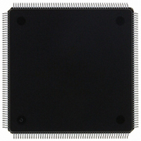
IC MPU 32BIT COLDF 90MHZ 208FQFP
Manufacturer
Freescale Semiconductor
Series
MCF530xr
Datasheets
1.MCF5307AI66B.pdf
(484 pages)
2.MCF5307AI66B.pdf
(16 pages)
3.MCF5307AI66B.pdf
(2 pages)
Specifications of MCF5307AI90B
Core Processor
Coldfire V3
Core Size
32-Bit
Speed
90MHz
Connectivity
EBI/EMI, I²C, UART/USART
Peripherals
DMA, POR, WDT
Number Of I /o
16
Program Memory Type
ROMless
Ram Size
4K x 8
Voltage - Supply (vcc/vdd)
3 V ~ 3.6 V
Oscillator Type
External
Operating Temperature
0°C ~ 70°C
Package / Case
208-FQFP
Maximum Clock Frequency
90 MHz
Maximum Operating Temperature
+ 105 C
Mounting Style
SMD/SMT
Minimum Operating Temperature
0 C
Family Name
MCF5xxx
Device Core
ColdFire
Device Core Size
32b
Frequency (max)
90MHz
Instruction Set Architecture
RISC
Supply Voltage 1 (typ)
3.3V
Operating Temp Range
0C to 70C
Operating Temperature Classification
Commercial
Mounting
Surface Mount
Pin Count
208
Package Type
FQFP
Program Memory Size
8KB
Cpu Speed
90MHz
Embedded Interface Type
I2C, UART
Digital Ic Case Style
FQFP
No. Of Pins
208
Supply Voltage Range
3V To 3.6V
Rohs Compliant
Yes
Lead Free Status / RoHS Status
Lead free / RoHS Compliant
Eeprom Size
-
Program Memory Size
-
Data Converters
-
Lead Free Status / Rohs Status
Lead free / RoHS Compliant
Available stocks
Company
Part Number
Manufacturer
Quantity
Price
Company:

Part Number:
MCF5307AI90B
Manufacturer:
FREESCAL
Quantity:
153
Company:
Part Number:
MCF5307AI90B
Manufacturer:
Freescale Semiconductor
Quantity:
10 000
Part Number:
MCF5307AI90B
Manufacturer:
FREESCALE
Quantity:
20 000


Chapter 16
Mechanical Data
This chapter provides a function pin listing and package diagram for the MCF5307. See the
website [http://www.motorola.com/coldfire] for any updated information.
16.1 Package
The MCF5307 is assembled in a 208-pin, thermally enhanced plastic QFP package.
16.2 Pinout
The MCF5307 pinout is detailed in the following tables, including the primary and
secondary functions of multiplexed signals. Additional columns indicate the output drive
capability of each pin, whether it is internally synchronized, and if the signal can change
on a negative clock transition.
These tables show MCF5307 pin numbers, including signal multiplexing. Additional
columns indicate the direction, description, and output drive capability of each pin.
No
10
11
12
1
2
3
4
5
6
7
8
9
Pin
Name
GND
GND
VCC
VCC
A0
A1
A2
A3
A4
A5
A6
A7
Table 16-1. Pins 1–52 (Left, Top-to-Bottom)
Freescale Semiconductor, Inc.
For More Information On This Product,
Alternate
Function
—
—
—
—
—
—
—
—
—
—
—
—
Chapter 16. Mechanical Data
Go to: www.freescale.com
I/O
I/O
I/O
I/O
I/O
I/O
I/O
I/O
I/O
—
—
—
—
Power input
Address bus bit
Address bus bit
Ground pin
Address bus bit
Address bus bit
Power input
Address bus bit
Address bus bit
Ground pin
Address bus bit
Address bus bit
Description
Drive
(mA)
—
—
—
—
8
8
8
8
8
8
8
8
16-1
Related parts for MCF5307AI90B
Image
Part Number
Description
Manufacturer
Datasheet
Request
R

Part Number:
Description:
Manufacturer:
Freescale Semiconductor, Inc
Datasheet:
Part Number:
Description:
Mcf5307 Coldfire Integrated Microprocessor User
Manufacturer:
Freescale Semiconductor, Inc
Datasheet:
Part Number:
Description:
Manufacturer:
Freescale Semiconductor, Inc
Datasheet:
Part Number:
Description:
Manufacturer:
Freescale Semiconductor, Inc
Datasheet:
Part Number:
Description:
Manufacturer:
Freescale Semiconductor, Inc
Datasheet:
Part Number:
Description:
Manufacturer:
Freescale Semiconductor, Inc
Datasheet:
Part Number:
Description:
Manufacturer:
Freescale Semiconductor, Inc
Datasheet:
Part Number:
Description:
Manufacturer:
Freescale Semiconductor, Inc
Datasheet:
Part Number:
Description:
Manufacturer:
Freescale Semiconductor, Inc
Datasheet:
Part Number:
Description:
Manufacturer:
Freescale Semiconductor, Inc
Datasheet:
Part Number:
Description:
Manufacturer:
Freescale Semiconductor, Inc
Datasheet:
Part Number:
Description:
Manufacturer:
Freescale Semiconductor, Inc
Datasheet:
Part Number:
Description:
Manufacturer:
Freescale Semiconductor, Inc
Datasheet:
Part Number:
Description:
Manufacturer:
Freescale Semiconductor, Inc
Datasheet:
Part Number:
Description:
Manufacturer:
Freescale Semiconductor, Inc
Datasheet: