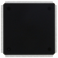
MCF5307AI90B Freescale Semiconductor, MCF5307AI90B Datasheet - Page 239

MCF5307AI90B
Manufacturer Part Number
MCF5307AI90B
Description
IC MPU 32BIT COLDF 90MHZ 208FQFP
Manufacturer
Freescale Semiconductor
Series
MCF530xr
Datasheets
1.MCF5307AI66B.pdf
(484 pages)
2.MCF5307AI66B.pdf
(16 pages)
3.MCF5307AI66B.pdf
(2 pages)
Specifications of MCF5307AI90B
Core Processor
Coldfire V3
Core Size
32-Bit
Speed
90MHz
Connectivity
EBI/EMI, I²C, UART/USART
Peripherals
DMA, POR, WDT
Number Of I /o
16
Program Memory Type
ROMless
Ram Size
4K x 8
Voltage - Supply (vcc/vdd)
3 V ~ 3.6 V
Oscillator Type
External
Operating Temperature
0°C ~ 70°C
Package / Case
208-FQFP
Maximum Clock Frequency
90 MHz
Maximum Operating Temperature
+ 105 C
Mounting Style
SMD/SMT
Minimum Operating Temperature
0 C
Family Name
MCF5xxx
Device Core
ColdFire
Device Core Size
32b
Frequency (max)
90MHz
Instruction Set Architecture
RISC
Supply Voltage 1 (typ)
3.3V
Operating Temp Range
0C to 70C
Operating Temperature Classification
Commercial
Mounting
Surface Mount
Pin Count
208
Package Type
FQFP
Program Memory Size
8KB
Cpu Speed
90MHz
Embedded Interface Type
I2C, UART
Digital Ic Case Style
FQFP
No. Of Pins
208
Supply Voltage Range
3V To 3.6V
Rohs Compliant
Yes
Lead Free Status / RoHS Status
Lead free / RoHS Compliant
Eeprom Size
-
Program Memory Size
-
Data Converters
-
Lead Free Status / Rohs Status
Lead free / RoHS Compliant
Available stocks
Company
Part Number
Manufacturer
Quantity
Price
Company:
Part Number:
MCF5307AI90B
Manufacturer:
FREESCAL
Quantity:
153
Company:
Part Number:
MCF5307AI90B
Manufacturer:
Freescale Semiconductor
Quantity:
10 000
Part Number:
MCF5307AI90B
Manufacturer:
FREESCALE
Quantity:
20 000
- Current page: 239 of 484
- Download datasheet (6Mb)
Table 11-3 describes DCR fields.
11.3.2.2 DRAM Address and Control Registers (DACR0/DACR1)
DACR0 and DACR1, Figure 11-3, contain the base address compare value and the control
bits for memory blocks 0 and 1. Address and timing are also controlled by these registers.
Memory areas defined for each block should not overlap; operation is undefined for
accesses in overlapping regions.
15
14
13
12–11
10–9
8–0
Address
Bits
Reset
Field SO
R/W
Name
NAM
RRA
RRP
SO
RC
—
15
Figure 11-2. DRAM Control Register (DCR) (Asynchronous Mode)
0
Synchronous operation. Selects synchronous or asynchronous mode. A DRAM controller in
synchronous mode can be switched to ADRAM mode only by resetting the MCF5307.
0 Asynchronous DRAMs. Default at reset.
1 Synchronous DRAMs
Reserved, should be cleared.
No address multiplexing. Some implementations require external multiplexing. For example, when
linear addressing is required, the DRAM should not multiplex addresses on DRAM accesses.
0 The DRAM controller multiplexes the external address bus to provide column addresses.
1 The DRAM controller does not multiplex the external address bus to provide column addresses.
Refresh RAS asserted. Determines how long RAS is asserted during a refresh operation.
00 2 clocks
01 3 clocks
10 4 clocks
11 5 clocks
Refresh RAS precharge. Controls how many clocks RAS is precharged after a refresh operation
before accesses are allowed to DRAM.
00 1 clock
01 2 clocks
10 3 clocks
11 4 clocks
Refresh count. Controls refresh frequency. The number of bus clocks between refresh cycles is
(RC + 1) * 16. Refresh can range from 16–8192 bus clocks to accommodate both standard and
low-power DRAMs with bus clock operation from less than 2 MHz to greater than 50 MHz.
The following example calculates RC for an auto-refresh period for 4096 rows to receive 64 mS of
refresh every 15.625 µs for each row (625 bus clocks at 40 MHz).
# of bus clocks = 625 = (RC field + 1) * 16
RC = (625 bus clocks/16) -1 = 38.06, which rounds to 38; therefore, RC = 0x26.
Table 11-3. DCR Field Descriptions (Asynchronous Mode)
14
—
NAM
13
Chapter 11. Synchronous/Asynchronous DRAM Controller Module
Freescale Semiconductor, Inc.
12
For More Information On This Product,
RRA
11
Go to: www.freescale.com
10
RRP
9
MBAR + 0x100
8
Uninitialized
Description
R/W
RC
Asynchronous Operation
11-5
0
Related parts for MCF5307AI90B
Image
Part Number
Description
Manufacturer
Datasheet
Request
R
Part Number:
Description:
Manufacturer:
Freescale Semiconductor, Inc
Datasheet:
Part Number:
Description:
Mcf5307 Coldfire Integrated Microprocessor User
Manufacturer:
Freescale Semiconductor, Inc
Datasheet:
Part Number:
Description:
Manufacturer:
Freescale Semiconductor, Inc
Datasheet:
Part Number:
Description:
Manufacturer:
Freescale Semiconductor, Inc
Datasheet:
Part Number:
Description:
Manufacturer:
Freescale Semiconductor, Inc
Datasheet:
Part Number:
Description:
Manufacturer:
Freescale Semiconductor, Inc
Datasheet:
Part Number:
Description:
Manufacturer:
Freescale Semiconductor, Inc
Datasheet:
Part Number:
Description:
Manufacturer:
Freescale Semiconductor, Inc
Datasheet:
Part Number:
Description:
Manufacturer:
Freescale Semiconductor, Inc
Datasheet:
Part Number:
Description:
Manufacturer:
Freescale Semiconductor, Inc
Datasheet:
Part Number:
Description:
Manufacturer:
Freescale Semiconductor, Inc
Datasheet:
Part Number:
Description:
Manufacturer:
Freescale Semiconductor, Inc
Datasheet:
Part Number:
Description:
Manufacturer:
Freescale Semiconductor, Inc
Datasheet:
Part Number:
Description:
Manufacturer:
Freescale Semiconductor, Inc
Datasheet:
Part Number:
Description:
Manufacturer:
Freescale Semiconductor, Inc
Datasheet:


