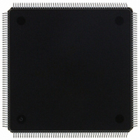
MCF5307AI90B Freescale Semiconductor, MCF5307AI90B Datasheet - Page 368

MCF5307AI90B
Manufacturer Part Number
MCF5307AI90B
Description
IC MPU 32BIT COLDF 90MHZ 208FQFP
Manufacturer
Freescale Semiconductor
Series
MCF530xr
Datasheets
1.MCF5307AI66B.pdf
(484 pages)
2.MCF5307AI66B.pdf
(16 pages)
3.MCF5307AI66B.pdf
(2 pages)
Specifications of MCF5307AI90B
Core Processor
Coldfire V3
Core Size
32-Bit
Speed
90MHz
Connectivity
EBI/EMI, I²C, UART/USART
Peripherals
DMA, POR, WDT
Number Of I /o
16
Program Memory Type
ROMless
Ram Size
4K x 8
Voltage - Supply (vcc/vdd)
3 V ~ 3.6 V
Oscillator Type
External
Operating Temperature
0°C ~ 70°C
Package / Case
208-FQFP
Maximum Clock Frequency
90 MHz
Maximum Operating Temperature
+ 105 C
Mounting Style
SMD/SMT
Minimum Operating Temperature
0 C
Family Name
MCF5xxx
Device Core
ColdFire
Device Core Size
32b
Frequency (max)
90MHz
Instruction Set Architecture
RISC
Supply Voltage 1 (typ)
3.3V
Operating Temp Range
0C to 70C
Operating Temperature Classification
Commercial
Mounting
Surface Mount
Pin Count
208
Package Type
FQFP
Program Memory Size
8KB
Cpu Speed
90MHz
Embedded Interface Type
I2C, UART
Digital Ic Case Style
FQFP
No. Of Pins
208
Supply Voltage Range
3V To 3.6V
Rohs Compliant
Yes
Lead Free Status / RoHS Status
Lead free / RoHS Compliant
Eeprom Size
-
Program Memory Size
-
Data Converters
-
Lead Free Status / Rohs Status
Lead free / RoHS Compliant
Available stocks
Company
Part Number
Manufacturer
Quantity
Price
Company:
Part Number:
MCF5307AI90B
Manufacturer:
FREESCAL
Quantity:
153
Company:
Part Number:
MCF5307AI90B
Manufacturer:
Freescale Semiconductor
Quantity:
10 000
Part Number:
MCF5307AI90B
Manufacturer:
FREESCALE
Quantity:
20 000
- Current page: 368 of 484
- Download datasheet (6Mb)
Overview
17-4
Frequency control PLL
Divide control PCLK to
BCLKO
Chip selects[7:0]
Byte enable[3:0]/
Byte write enable[3:0]
Output enable
Row address strobe
Column address strobe
DRAM write
Synchronous column
address strobe
Synchronous row
address strobe
Synchronous clock
enable
Synchronous edge
select
DMA request
Receive data
Transmit data
Request-to-send
Clear-to-send
Timer input
Timer outputs
Signal Name
Table 17-1. MCF5307 Signal Index (Continued)
FREQ[1:0]
DIVIDE[1:0]
CS[7:0]
BE[3:0]/
BWE[3:0]
OE
RAS[1:0]
CAS[3:0]
DRAMW
SCAS
SRAS
SCKE
EDGESEL
DREQ[1:0]
RxD[1:0]
TxD[1:0]
RTS[1:0]
CTS[1:0]
TIN[1:0]
TOUT[1:0]
Abbreviation
Section 17.8, “DMA Controller Module Signals”
Freescale Semiconductor, Inc.
Section 17.6, “Chip-Select Module Signals”
Section 17.11, “Parallel I/O Port (PP[15:0])”
Section 17.7, “DRAM Controller Signals”
For More Information On This Product,
Section 17.10, “Timer Module Signals”
Section 17.9, “Serial Module Signals”
Go to: www.freescale.com
MCF5307 User’s Manual
Indicates CLKIN frequency range.
Indicates the BCLKO/PSTCLK ratio.
Enables peripherals at programmed
addresses; CS0 provides boot ROM
selection.
BE[3:0] select bytes in memory.
Output enable for chip select read
cycles
DRAM row address strobe
DRAM column address strobe
Asserted for DRAM write; negated
for DRAM read
SDRAM column address strobe
SDRAM row address strobe
Clock enable for external SDRAM
Timing select for external SDRAM
External DMA transfer request;
multiplexed with PP[6:5]
Receive serial data input for UART
Transmit serial data output for UART
UART asserts when ready to
receive data query.
Signals UART that data can be sent
to peripheral
Clock input to timer or trigger to
timer value capture logic
Outputs waveform or pulse.
Function
I/O
O
O
O
O
O
O
O
O
O
O
O
O
I
I
I
I
I
I
I
Reset
High
High
High
High
High
High
High
High
High
High
High
Low
—
—
—
—
—
User cfg 17-17
Pull-Up Page
17-15
17-15
17-15
17-16
17-16
17-16
17-16
17-16
17-16
17-17
17-17
17-17
17-17
17-17
17-18
17-18
17-18
17-18
17-18
17-18
17-18
17-19
17-19
17-19
Related parts for MCF5307AI90B
Image
Part Number
Description
Manufacturer
Datasheet
Request
R
Part Number:
Description:
Manufacturer:
Freescale Semiconductor, Inc
Datasheet:
Part Number:
Description:
Mcf5307 Coldfire Integrated Microprocessor User
Manufacturer:
Freescale Semiconductor, Inc
Datasheet:
Part Number:
Description:
Manufacturer:
Freescale Semiconductor, Inc
Datasheet:
Part Number:
Description:
Manufacturer:
Freescale Semiconductor, Inc
Datasheet:
Part Number:
Description:
Manufacturer:
Freescale Semiconductor, Inc
Datasheet:
Part Number:
Description:
Manufacturer:
Freescale Semiconductor, Inc
Datasheet:
Part Number:
Description:
Manufacturer:
Freescale Semiconductor, Inc
Datasheet:
Part Number:
Description:
Manufacturer:
Freescale Semiconductor, Inc
Datasheet:
Part Number:
Description:
Manufacturer:
Freescale Semiconductor, Inc
Datasheet:
Part Number:
Description:
Manufacturer:
Freescale Semiconductor, Inc
Datasheet:
Part Number:
Description:
Manufacturer:
Freescale Semiconductor, Inc
Datasheet:
Part Number:
Description:
Manufacturer:
Freescale Semiconductor, Inc
Datasheet:
Part Number:
Description:
Manufacturer:
Freescale Semiconductor, Inc
Datasheet:
Part Number:
Description:
Manufacturer:
Freescale Semiconductor, Inc
Datasheet:
Part Number:
Description:
Manufacturer:
Freescale Semiconductor, Inc
Datasheet:


