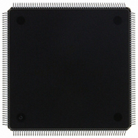
MCF5307AI90B Freescale Semiconductor, MCF5307AI90B Datasheet - Page 242

MCF5307AI90B
Manufacturer Part Number
MCF5307AI90B
Description
IC MPU 32BIT COLDF 90MHZ 208FQFP
Manufacturer
Freescale Semiconductor
Series
MCF530xr
Datasheets
1.MCF5307AI66B.pdf
(484 pages)
2.MCF5307AI66B.pdf
(16 pages)
3.MCF5307AI66B.pdf
(2 pages)
Specifications of MCF5307AI90B
Core Processor
Coldfire V3
Core Size
32-Bit
Speed
90MHz
Connectivity
EBI/EMI, I²C, UART/USART
Peripherals
DMA, POR, WDT
Number Of I /o
16
Program Memory Type
ROMless
Ram Size
4K x 8
Voltage - Supply (vcc/vdd)
3 V ~ 3.6 V
Oscillator Type
External
Operating Temperature
0°C ~ 70°C
Package / Case
208-FQFP
Maximum Clock Frequency
90 MHz
Maximum Operating Temperature
+ 105 C
Mounting Style
SMD/SMT
Minimum Operating Temperature
0 C
Family Name
MCF5xxx
Device Core
ColdFire
Device Core Size
32b
Frequency (max)
90MHz
Instruction Set Architecture
RISC
Supply Voltage 1 (typ)
3.3V
Operating Temp Range
0C to 70C
Operating Temperature Classification
Commercial
Mounting
Surface Mount
Pin Count
208
Package Type
FQFP
Program Memory Size
8KB
Cpu Speed
90MHz
Embedded Interface Type
I2C, UART
Digital Ic Case Style
FQFP
No. Of Pins
208
Supply Voltage Range
3V To 3.6V
Rohs Compliant
Yes
Lead Free Status / RoHS Status
Lead free / RoHS Compliant
Eeprom Size
-
Program Memory Size
-
Data Converters
-
Lead Free Status / Rohs Status
Lead free / RoHS Compliant
Available stocks
Company
Part Number
Manufacturer
Quantity
Price
Company:
Part Number:
MCF5307AI90B
Manufacturer:
FREESCAL
Quantity:
153
Company:
Part Number:
MCF5307AI90B
Manufacturer:
Freescale Semiconductor
Quantity:
10 000
Part Number:
MCF5307AI90B
Manufacturer:
FREESCALE
Quantity:
20 000
- Current page: 242 of 484
- Download datasheet (6Mb)
Asynchronous Operation
11.3.3 General Asynchronous Operation Guidelines
The DRAM controller provides control for RAS, CAS, and DRAMW signals, as well as
address multiplexing and bus cycle termination. Whether the mode is synchronous or
asynchronous determines signal control and termination. To reduce complexity,
multiplexing is the same for both modes. Table 11-6 shows the scheme for DRAM
configurations. This scheme works for symmetric configurations (in which the number of
rows equals the number of columns) as well as asymmetric configurations (in which the
number of rows and columns are different).
11-8
Bits
6–1
Address Pin
0
17
16
15
14
13
12
11
10
17
18
19
9
Name
AMx
V
Row Address
Address modifier masks. Determine which accesses can occur in a given DRAM block.
0 Allow access type to hit in DRAM
1 Do not allow access type to hit in DRAM
Valid. Cleared at reset to ensure that the DRAM block is not erroneously decoded.
0 Do not decode DRAM accesses.
1 Registers controlling the DRAM block are initialized; DRAM accesses can be decoded.
Table 11-5. DMR0/DMR1 Field Descriptions (Continued)
AM
SC
SD
UC
UD
Bit
C/I
17
16
15
14
13
12
11
10
17
18
19
Table 11-6. Generic Address Multiplexing Scheme
9
CPU space/interrupt acknowledge
Alternate master
Supervisor code
Supervisor data
User code
User data
Freescale Semiconductor, Inc.
Associated Access Type
For More Information On This Product,
Column Address
16
17
18
0
1
2
3
4
5
6
7
8
Go to: www.freescale.com
MCF5307 User’s Manual
8-bit port only
8- and 16-bit ports only
32-bit port only
16-bit port only or 32-bit port with only 8 column address lines
16-bit port only when at least 9 column address lines are used
Description
MOVEC instruction or interrupt acknowledge cycle
External or DMA master
Any supervisor-only instruction access
Any data fetched during the instruction access
Any user instruction
Any user data
Notes Relating to Port Sizes
Access Definition
Related parts for MCF5307AI90B
Image
Part Number
Description
Manufacturer
Datasheet
Request
R
Part Number:
Description:
Manufacturer:
Freescale Semiconductor, Inc
Datasheet:
Part Number:
Description:
Mcf5307 Coldfire Integrated Microprocessor User
Manufacturer:
Freescale Semiconductor, Inc
Datasheet:
Part Number:
Description:
Manufacturer:
Freescale Semiconductor, Inc
Datasheet:
Part Number:
Description:
Manufacturer:
Freescale Semiconductor, Inc
Datasheet:
Part Number:
Description:
Manufacturer:
Freescale Semiconductor, Inc
Datasheet:
Part Number:
Description:
Manufacturer:
Freescale Semiconductor, Inc
Datasheet:
Part Number:
Description:
Manufacturer:
Freescale Semiconductor, Inc
Datasheet:
Part Number:
Description:
Manufacturer:
Freescale Semiconductor, Inc
Datasheet:
Part Number:
Description:
Manufacturer:
Freescale Semiconductor, Inc
Datasheet:
Part Number:
Description:
Manufacturer:
Freescale Semiconductor, Inc
Datasheet:
Part Number:
Description:
Manufacturer:
Freescale Semiconductor, Inc
Datasheet:
Part Number:
Description:
Manufacturer:
Freescale Semiconductor, Inc
Datasheet:
Part Number:
Description:
Manufacturer:
Freescale Semiconductor, Inc
Datasheet:
Part Number:
Description:
Manufacturer:
Freescale Semiconductor, Inc
Datasheet:
Part Number:
Description:
Manufacturer:
Freescale Semiconductor, Inc
Datasheet:


