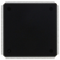
MCF5307AI90B Freescale Semiconductor, MCF5307AI90B Datasheet - Page 292

MCF5307AI90B
Manufacturer Part Number
MCF5307AI90B
Description
IC MPU 32BIT COLDF 90MHZ 208FQFP
Manufacturer
Freescale Semiconductor
Series
MCF530xr
Datasheets
1.MCF5307AI66B.pdf
(484 pages)
2.MCF5307AI66B.pdf
(16 pages)
3.MCF5307AI66B.pdf
(2 pages)
Specifications of MCF5307AI90B
Core Processor
Coldfire V3
Core Size
32-Bit
Speed
90MHz
Connectivity
EBI/EMI, I²C, UART/USART
Peripherals
DMA, POR, WDT
Number Of I /o
16
Program Memory Type
ROMless
Ram Size
4K x 8
Voltage - Supply (vcc/vdd)
3 V ~ 3.6 V
Oscillator Type
External
Operating Temperature
0°C ~ 70°C
Package / Case
208-FQFP
Maximum Clock Frequency
90 MHz
Maximum Operating Temperature
+ 105 C
Mounting Style
SMD/SMT
Minimum Operating Temperature
0 C
Family Name
MCF5xxx
Device Core
ColdFire
Device Core Size
32b
Frequency (max)
90MHz
Instruction Set Architecture
RISC
Supply Voltage 1 (typ)
3.3V
Operating Temp Range
0C to 70C
Operating Temperature Classification
Commercial
Mounting
Surface Mount
Pin Count
208
Package Type
FQFP
Program Memory Size
8KB
Cpu Speed
90MHz
Embedded Interface Type
I2C, UART
Digital Ic Case Style
FQFP
No. Of Pins
208
Supply Voltage Range
3V To 3.6V
Rohs Compliant
Yes
Lead Free Status / RoHS Status
Lead free / RoHS Compliant
Eeprom Size
-
Program Memory Size
-
Data Converters
-
Lead Free Status / Rohs Status
Lead free / RoHS Compliant
Available stocks
Company
Part Number
Manufacturer
Quantity
Price
Company:
Part Number:
MCF5307AI90B
Manufacturer:
FREESCAL
Quantity:
153
Company:
Part Number:
MCF5307AI90B
Manufacturer:
Freescale Semiconductor
Quantity:
10 000
Part Number:
MCF5307AI90B
Manufacturer:
FREESCALE
Quantity:
20 000
- Current page: 292 of 484
- Download datasheet (6Mb)
Freescale Semiconductor, Inc.
DMA Controller Module Functional Description
is from memory to either a peripheral device or memory, the source address is the starting
address of the data block. This can be any aligned byte address. In single-address mode, this
data register is used regardless of transfer direction.
The DAR should contain the destination (write) address. If the transfer is from a peripheral
device to memory, or memory to memory, the DAR is loaded with the starting address of
the data block to be written. If the transfer is from memory to a peripheral device, DAR is
loaded with the address of the peripheral data register. This address can be any aligned byte
address. DAR is not used in single-address mode.
SAR and DAR change after each cycle depending on DCR[SSIZE,DSIZE,SINC,DINC]
and on the starting address. Increment values can be 1, 2, 4, or 16 for byte, word, longword,
or line transfers, respectively. If the address register is programmed to remain unchanged
(no count), the register is not incremented after the data transfer.
BCRn[BCR] must be loaded with the number of byte transfers to occur. It is decremented
by 1, 2, 4, or 16 at the end of each transfer, depending on the transfer size. DSR must be
cleared for channel startup.
As soon as the channel has been initialized, it is started by writing a one to DCR[START]
or asserting DREQ, depending on the status of DCR[EEXT]. Programming the channel for
internal request causes the channel to request the bus and start transferring data
immediately. If the channel is programmed for external request, DREQ must be asserted
before the channel requests the bus.
Changes to DCR are effective immediately while the channel is active. To avoid problems
with changing a DMA channel setup, write a one to DSR[DONE] to stop the DMA channel.
12.5.4 Data Transfer
This section includes timing diagrams that illustrate the interaction of signals in DMA data
transfers. It also describes auto-alignment and bandwidth control.
12.5.4.1 External Request and Acknowledge Operation
Channels 0 and 1 initiate transfers to an external module by means of DREQ[1:0]. The
request for channels 2 and 3 are connected internally to the UART0 and UART1 interrupt
signals, respectively. If DCR[EEXT] = 1 and the channel is idle, the DMA initiates a
transfer when DREQ is asserted.
Figure 12-11 shows the minimum 4-clock cycle delay from when DREQ is sampled
asserted to when a DMA bus cycle begins. This delay may be longer, depending on DMA
priority, bus arbitration, DRAM refresh operations, and other factors.
12-14
MCF5307 User’s Manual
For More Information On This Product,
Go to: www.freescale.com
Related parts for MCF5307AI90B
Image
Part Number
Description
Manufacturer
Datasheet
Request
R
Part Number:
Description:
Manufacturer:
Freescale Semiconductor, Inc
Datasheet:
Part Number:
Description:
Mcf5307 Coldfire Integrated Microprocessor User
Manufacturer:
Freescale Semiconductor, Inc
Datasheet:
Part Number:
Description:
Manufacturer:
Freescale Semiconductor, Inc
Datasheet:
Part Number:
Description:
Manufacturer:
Freescale Semiconductor, Inc
Datasheet:
Part Number:
Description:
Manufacturer:
Freescale Semiconductor, Inc
Datasheet:
Part Number:
Description:
Manufacturer:
Freescale Semiconductor, Inc
Datasheet:
Part Number:
Description:
Manufacturer:
Freescale Semiconductor, Inc
Datasheet:
Part Number:
Description:
Manufacturer:
Freescale Semiconductor, Inc
Datasheet:
Part Number:
Description:
Manufacturer:
Freescale Semiconductor, Inc
Datasheet:
Part Number:
Description:
Manufacturer:
Freescale Semiconductor, Inc
Datasheet:
Part Number:
Description:
Manufacturer:
Freescale Semiconductor, Inc
Datasheet:
Part Number:
Description:
Manufacturer:
Freescale Semiconductor, Inc
Datasheet:
Part Number:
Description:
Manufacturer:
Freescale Semiconductor, Inc
Datasheet:
Part Number:
Description:
Manufacturer:
Freescale Semiconductor, Inc
Datasheet:
Part Number:
Description:
Manufacturer:
Freescale Semiconductor, Inc
Datasheet:


