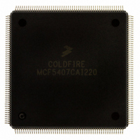
MCF5407CAI220 Freescale Semiconductor, MCF5407CAI220 Datasheet - Page 181

MCF5407CAI220
Manufacturer Part Number
MCF5407CAI220
Description
IC MPU 32B 220MHZ COLDF 208-FQFP
Manufacturer
Freescale Semiconductor
Series
MCF540xr
Specifications of MCF5407CAI220
Core Processor
Coldfire V4
Core Size
32-Bit
Speed
220MHz
Connectivity
EBI/EMI, I²C, UART/USART
Peripherals
DMA, WDT
Number Of I /o
16
Program Memory Type
ROMless
Ram Size
4K x 8
Voltage - Supply (vcc/vdd)
1.65 V ~ 3.6 V
Oscillator Type
External
Operating Temperature
-40°C ~ 85°C
Package / Case
208-FQFP
Processor Series
MCF540x
Core
ColdFire V4
Data Bus Width
32 bit
Program Memory Size
8 KB
Data Ram Size
4 KB
Maximum Clock Frequency
162 MHz
Number Of Programmable I/os
16
Operating Supply Voltage
1.8 V to 3.3 V
Mounting Style
SMD/SMT
3rd Party Development Tools
JLINK-CF-BDM26, EWCF
Cpu Speed
220MHz
Embedded Interface Type
I2C, UART
Digital Ic Case Style
FQFP
No. Of Pins
208
Supply Voltage Range
3.3V
Rohs Compliant
Yes
For Use With
M5407C3 - KIT EVAL FOR MCF5407 W/ETHERNET
Lead Free Status / RoHS Status
Lead free / RoHS Compliant
Eeprom Size
-
Program Memory Size
-
Data Converters
-
Lead Free Status / Rohs Status
Lead free / RoHS Compliant
Available stocks
Company
Part Number
Manufacturer
Quantity
Price
Company:
Part Number:
MCF5407CAI220
Manufacturer:
Freescale
Quantity:
789
Company:
Part Number:
MCF5407CAI220
Manufacturer:
Freescale Semiconductor
Quantity:
10 000
- Current page: 181 of 546
- Download datasheet (7Mb)
DSCLK and DSI are synchronized inputs. DSCLK acts as a pseudo clock enable and is
sampled on the rising edge of the processor CLK as well as the DSI. DSO is delayed from
the DSCLK-enabled CLK rising edge (registered after a BDM state machine state change).
All events in the debug module’s serial state machine are based on the processor clock
rising edge. DSCLK must also be sampled low (on a positive edge of CLK) between each
bit exchange. The MSB is transferred first. Because DSO changes state based on an
internally-recognized rising edge of DSCLK, DSDO cannot be used to indicate the start of
a serial transfer. The development system must count clock cycles in a given transfer.
C1–C4 are described as follows:
5.5.2.1 Receive Packet Format
The basic receive packet, Figure 5-16, consists of 16 data bits and 1 status bit.
Table 5-19 describes receive BDM packet fields.
16
15–0 Data
Bits
16
S
• C1—First synchronization cycle for DSI (DSCLK is high).
• C2—Second synchronization cycle for DSI (DSCLK is high).
• C3—BDM state machine changes state depending upon DSI and whether the entire
• C4—DSO changes to next value.
S
Name
15
input data transfer has been transmitted.
Status. Indicates the status of CPU-generated messages listed below. The not-ready response can
be ignored unless a memory-referencing cycle is in progress. Otherwise, the debug module can
accept a new serial transfer after 32 processor clock periods.
S
0
0
1
1
1
Data. Contains the message to be sent from the debug module to the development system. The
response message is always a single word, with the data field encoded as shown above.
A not-ready response can be ignored except during a
memory-referencing cycle. Otherwise, the debug module can
accept a new serial transfer after 32 processor clock periods.
Data
xxxx
0xFFFF
0x0000
0x0001
0xFFFF
Table 5-19. Receive BDM Packet Field Description
Message
Valid data transfer
Status OK
Not ready with response; come again
Error—Terminated bus cycle; data invalid
Illegal command
Figure 5-16. Receive BDM Packet
Chapter 5. Debug Support
NOTE:
Data Field [15:0]
Description
Background Debug Mode (BDM)
5-25
0
Related parts for MCF5407CAI220
Image
Part Number
Description
Manufacturer
Datasheet
Request
R
Part Number:
Description:
Mcf5407 Coldfire Integrated Microprocessor User
Manufacturer:
Freescale Semiconductor, Inc
Datasheet:
Part Number:
Description:
Manufacturer:
Freescale Semiconductor, Inc
Datasheet:
Part Number:
Description:
Manufacturer:
Freescale Semiconductor, Inc
Datasheet:
Part Number:
Description:
Manufacturer:
Freescale Semiconductor, Inc
Datasheet:
Part Number:
Description:
Manufacturer:
Freescale Semiconductor, Inc
Datasheet:
Part Number:
Description:
Manufacturer:
Freescale Semiconductor, Inc
Datasheet:
Part Number:
Description:
Manufacturer:
Freescale Semiconductor, Inc
Datasheet:
Part Number:
Description:
Manufacturer:
Freescale Semiconductor, Inc
Datasheet:
Part Number:
Description:
Manufacturer:
Freescale Semiconductor, Inc
Datasheet:
Part Number:
Description:
Manufacturer:
Freescale Semiconductor, Inc
Datasheet:
Part Number:
Description:
Manufacturer:
Freescale Semiconductor, Inc
Datasheet:
Part Number:
Description:
Manufacturer:
Freescale Semiconductor, Inc
Datasheet:
Part Number:
Description:
Manufacturer:
Freescale Semiconductor, Inc
Datasheet:
Part Number:
Description:
Manufacturer:
Freescale Semiconductor, Inc
Datasheet:
Part Number:
Description:
Manufacturer:
Freescale Semiconductor, Inc
Datasheet:


