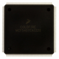
MCF5407CAI220 Freescale Semiconductor, MCF5407CAI220 Datasheet - Page 431

MCF5407CAI220
Manufacturer Part Number
MCF5407CAI220
Description
IC MPU 32B 220MHZ COLDF 208-FQFP
Manufacturer
Freescale Semiconductor
Series
MCF540xr
Specifications of MCF5407CAI220
Core Processor
Coldfire V4
Core Size
32-Bit
Speed
220MHz
Connectivity
EBI/EMI, I²C, UART/USART
Peripherals
DMA, WDT
Number Of I /o
16
Program Memory Type
ROMless
Ram Size
4K x 8
Voltage - Supply (vcc/vdd)
1.65 V ~ 3.6 V
Oscillator Type
External
Operating Temperature
-40°C ~ 85°C
Package / Case
208-FQFP
Processor Series
MCF540x
Core
ColdFire V4
Data Bus Width
32 bit
Program Memory Size
8 KB
Data Ram Size
4 KB
Maximum Clock Frequency
162 MHz
Number Of Programmable I/os
16
Operating Supply Voltage
1.8 V to 3.3 V
Mounting Style
SMD/SMT
3rd Party Development Tools
JLINK-CF-BDM26, EWCF
Cpu Speed
220MHz
Embedded Interface Type
I2C, UART
Digital Ic Case Style
FQFP
No. Of Pins
208
Supply Voltage Range
3.3V
Rohs Compliant
Yes
For Use With
M5407C3 - KIT EVAL FOR MCF5407 W/ETHERNET
Lead Free Status / RoHS Status
Lead free / RoHS Compliant
Eeprom Size
-
Program Memory Size
-
Data Converters
-
Lead Free Status / Rohs Status
Lead free / RoHS Compliant
Available stocks
Company
Part Number
Manufacturer
Quantity
Price
Company:
Part Number:
MCF5407CAI220
Manufacturer:
Freescale
Quantity:
789
Company:
Part Number:
MCF5407CAI220
Manufacturer:
Freescale Semiconductor
Quantity:
10 000
- Current page: 431 of 546
- Download datasheet (7Mb)
The address bus, write data, TS, and all attribute signals change on the rising edge of
CLKIN. Read data is latched into the MCF5407 on the rising edge of CLKIN. AS, CSx,
OE, and BE/BWE change on the falling edge.
The MCF5407 bus supports byte, word, and longword operand transfers and allows
accesses to 8-, 16-, and 32-bit data ports. Transfer parameters such as port size, the number
of wait states for the external slave being accessed, and whether internal transfer
termination is enabled, can be programmed in the chip-select control registers (CSCRs) and
DRAM control registers (DACRs).
For aligned transfers larger than the port size, SIZ[1:0] behaves as follows:
Table 18-2 shows encoding for SIZ[1:0].
Figure 18-2 shows the byte lanes that external memory should be connected to and the
sequential transfers if a longword is transferred for three port sizes. For example, an 8-bit
memory should be connected to D[31:24] (BE0). A longword transfer takes four transfers
on D[31:24], starting with the MSB and going to the LSB.
• Address bus (A[31:0])
• Data bus (D[31:0])
• Control signals (TS and TA)
• AS, CSx, OE, BE/BWE
• Attribute signals (R/W, SIZ, TT, TM, and TIP)
• If bursting is used, SIZ[1:0] stays at the size of transfer.
• If bursting is inhibited, SIZ[1:0] first shows the size of the transfer and then shows
the port size.
Table 18-2. Bus Cycle Size Encoding
00
01
10
11
Chapter 18. Bus Operation
SIZ[1:0]
Longword
Byte
Word
Line
Port Size
Data Transfer Operation
18-3
Related parts for MCF5407CAI220
Image
Part Number
Description
Manufacturer
Datasheet
Request
R
Part Number:
Description:
Mcf5407 Coldfire Integrated Microprocessor User
Manufacturer:
Freescale Semiconductor, Inc
Datasheet:
Part Number:
Description:
Manufacturer:
Freescale Semiconductor, Inc
Datasheet:
Part Number:
Description:
Manufacturer:
Freescale Semiconductor, Inc
Datasheet:
Part Number:
Description:
Manufacturer:
Freescale Semiconductor, Inc
Datasheet:
Part Number:
Description:
Manufacturer:
Freescale Semiconductor, Inc
Datasheet:
Part Number:
Description:
Manufacturer:
Freescale Semiconductor, Inc
Datasheet:
Part Number:
Description:
Manufacturer:
Freescale Semiconductor, Inc
Datasheet:
Part Number:
Description:
Manufacturer:
Freescale Semiconductor, Inc
Datasheet:
Part Number:
Description:
Manufacturer:
Freescale Semiconductor, Inc
Datasheet:
Part Number:
Description:
Manufacturer:
Freescale Semiconductor, Inc
Datasheet:
Part Number:
Description:
Manufacturer:
Freescale Semiconductor, Inc
Datasheet:
Part Number:
Description:
Manufacturer:
Freescale Semiconductor, Inc
Datasheet:
Part Number:
Description:
Manufacturer:
Freescale Semiconductor, Inc
Datasheet:
Part Number:
Description:
Manufacturer:
Freescale Semiconductor, Inc
Datasheet:
Part Number:
Description:
Manufacturer:
Freescale Semiconductor, Inc
Datasheet:


