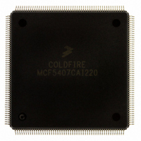
MCF5407CAI220 Freescale Semiconductor, MCF5407CAI220 Datasheet - Page 288

MCF5407CAI220
Manufacturer Part Number
MCF5407CAI220
Description
IC MPU 32B 220MHZ COLDF 208-FQFP
Manufacturer
Freescale Semiconductor
Series
MCF540xr
Specifications of MCF5407CAI220
Core Processor
Coldfire V4
Core Size
32-Bit
Speed
220MHz
Connectivity
EBI/EMI, I²C, UART/USART
Peripherals
DMA, WDT
Number Of I /o
16
Program Memory Type
ROMless
Ram Size
4K x 8
Voltage - Supply (vcc/vdd)
1.65 V ~ 3.6 V
Oscillator Type
External
Operating Temperature
-40°C ~ 85°C
Package / Case
208-FQFP
Processor Series
MCF540x
Core
ColdFire V4
Data Bus Width
32 bit
Program Memory Size
8 KB
Data Ram Size
4 KB
Maximum Clock Frequency
162 MHz
Number Of Programmable I/os
16
Operating Supply Voltage
1.8 V to 3.3 V
Mounting Style
SMD/SMT
3rd Party Development Tools
JLINK-CF-BDM26, EWCF
Cpu Speed
220MHz
Embedded Interface Type
I2C, UART
Digital Ic Case Style
FQFP
No. Of Pins
208
Supply Voltage Range
3.3V
Rohs Compliant
Yes
For Use With
M5407C3 - KIT EVAL FOR MCF5407 W/ETHERNET
Lead Free Status / RoHS Status
Lead free / RoHS Compliant
Eeprom Size
-
Program Memory Size
-
Data Converters
-
Lead Free Status / Rohs Status
Lead free / RoHS Compliant
Available stocks
Company
Part Number
Manufacturer
Quantity
Price
Company:
Part Number:
MCF5407CAI220
Manufacturer:
Freescale
Quantity:
789
Company:
Part Number:
MCF5407CAI220
Manufacturer:
Freescale Semiconductor
Quantity:
10 000
- Current page: 288 of 546
- Download datasheet (7Mb)
Synchronous Operation
11.4.3.2 DRAM Address and Control Registers (DACR0/DACR1) in
The DRAM address and control registers (DACR0 and DACR1), shown in Figure 11-16,
contain the base address compare value and the control bits for both memory blocks 0 and
1 of the DRAM controller. Address and timing are also controlled by bits in DACRn.
11-20
10–9
Reset
Bits
8–0
Field
Addr
12
11
R/W
31
Name
Table 11-12. DCR Field Descriptions (Synchronous Mode) (Continued)
RTIM
COC
RC
IS
Figure 11-16. DACR0 and DACR1 Registers (Synchronous Mode)
Synchronous Mode
Command on SDRAM clock enable (SCKE). Implementations that use external multiplexing
(NAM = 1) must support command information to be multiplexed onto the SDRAM address bus.
0 SCKE functions as a clock enable; self-refresh is initiated by the DRAM controller through DCR[IS].
1 SCKE drives command information. Because SCKE is not a clock enable, self-refresh cannot be
Initiate self-refresh command.
0 Take no action or issue a
1 If DCR[COC] = 0, the DRAM controller sends a
Refresh timing. Determines the timing operation of auto-refresh in the DRAM controller. Specifically,
it determines the number of clocks inserted between a
command. This same timing is used for both memory blocks controlled by the DRAM controller. This
corresponds to t
00 3 clocks
01 6 clocks
1x 9 clocks
Refresh count. Controls refresh frequency. The number of bus clocks between refresh cycles is
(RC + 1) * 16. Refresh can range from 16–8192 bus clocks to accommodate both standard and
low-power DRAMs with bus clock operation from less than 2 MHz to greater than 50 MHz.
The following example calculates RC for an auto-refresh period for 4096 rows to receive 64 mS of
refresh every 15.625 µs for each row (625 bus clocks at 40 MHz). This operation is the same as in
asynchronous mode.
# of bus clocks = 625 = (RC field + 1) * 16
RC = (625 bus clocks/16) -1 = 38.06, which rounds to 38; therefore, RC = 0x26.
used (setting DCR[IS]). Thus, external logic must be used if this functionality is desired. External
multiplexing is also responsible for putting the command information on the proper address bit.
in low-power, self-refresh state where they remain until IS is cleared, at which point the controller
sends a
while the SDRAMs are in self-refresh; the SDRAM controls the refresh period.
Uninitialized
BA
SELFX
RC
command for the SDRAMs to exit self-refresh. The refresh counter is suspended
in the SDRAM specifications.
18
MBAR+0x108 (DACR0); 0x110(DACR1)
SELFX
MCF5407 User’s Manual
17
—
16
command to exit self refresh.
RE
15
0
R/W
Description
—
14
13
CASL —
SELF
Uninitialized
12
command to both SDRAM blocks to put them
REF
11
command and the next possible
10
CBM
9
8
— IMRS
7
0
6
5
PS
Uninitialized
4
IP PM —
3
ACTV
2
1 0
Related parts for MCF5407CAI220
Image
Part Number
Description
Manufacturer
Datasheet
Request
R
Part Number:
Description:
Mcf5407 Coldfire Integrated Microprocessor User
Manufacturer:
Freescale Semiconductor, Inc
Datasheet:
Part Number:
Description:
Manufacturer:
Freescale Semiconductor, Inc
Datasheet:
Part Number:
Description:
Manufacturer:
Freescale Semiconductor, Inc
Datasheet:
Part Number:
Description:
Manufacturer:
Freescale Semiconductor, Inc
Datasheet:
Part Number:
Description:
Manufacturer:
Freescale Semiconductor, Inc
Datasheet:
Part Number:
Description:
Manufacturer:
Freescale Semiconductor, Inc
Datasheet:
Part Number:
Description:
Manufacturer:
Freescale Semiconductor, Inc
Datasheet:
Part Number:
Description:
Manufacturer:
Freescale Semiconductor, Inc
Datasheet:
Part Number:
Description:
Manufacturer:
Freescale Semiconductor, Inc
Datasheet:
Part Number:
Description:
Manufacturer:
Freescale Semiconductor, Inc
Datasheet:
Part Number:
Description:
Manufacturer:
Freescale Semiconductor, Inc
Datasheet:
Part Number:
Description:
Manufacturer:
Freescale Semiconductor, Inc
Datasheet:
Part Number:
Description:
Manufacturer:
Freescale Semiconductor, Inc
Datasheet:
Part Number:
Description:
Manufacturer:
Freescale Semiconductor, Inc
Datasheet:
Part Number:
Description:
Manufacturer:
Freescale Semiconductor, Inc
Datasheet:


