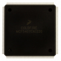
MCF5407CAI220 Freescale Semiconductor, MCF5407CAI220 Datasheet - Page 26
MCF5407CAI220
Manufacturer Part Number
MCF5407CAI220
Description
IC MPU 32B 220MHZ COLDF 208-FQFP
Manufacturer
Freescale Semiconductor
Series
MCF540xr
Specifications of MCF5407CAI220
Core Processor
Coldfire V4
Core Size
32-Bit
Speed
220MHz
Connectivity
EBI/EMI, I²C, UART/USART
Peripherals
DMA, WDT
Number Of I /o
16
Program Memory Type
ROMless
Ram Size
4K x 8
Voltage - Supply (vcc/vdd)
1.65 V ~ 3.6 V
Oscillator Type
External
Operating Temperature
-40°C ~ 85°C
Package / Case
208-FQFP
Processor Series
MCF540x
Core
ColdFire V4
Data Bus Width
32 bit
Program Memory Size
8 KB
Data Ram Size
4 KB
Maximum Clock Frequency
162 MHz
Number Of Programmable I/os
16
Operating Supply Voltage
1.8 V to 3.3 V
Mounting Style
SMD/SMT
3rd Party Development Tools
JLINK-CF-BDM26, EWCF
Cpu Speed
220MHz
Embedded Interface Type
I2C, UART
Digital Ic Case Style
FQFP
No. Of Pins
208
Supply Voltage Range
3.3V
Rohs Compliant
Yes
For Use With
M5407C3 - KIT EVAL FOR MCF5407 W/ETHERNET
Lead Free Status / RoHS Status
Lead free / RoHS Compliant
Eeprom Size
-
Program Memory Size
-
Data Converters
-
Lead Free Status / Rohs Status
Lead free / RoHS Compliant
Available stocks
Company
Part Number
Manufacturer
Quantity
Price
Company:

Part Number:
MCF5407CAI220
Manufacturer:
Freescale
Quantity:
789
Company:
Part Number:
MCF5407CAI220
Manufacturer:
Freescale Semiconductor
Quantity:
10 000


Figure
Number
18-1
18-2
18-3
18-4
18-5
18-6
18-7
18-8
18-9
18-10
18-11
18-12
18-13
18-14
18-15
18-16
18-17
18-18
18-19
18-20
18-21
18-22
18-23
18-24
18-25
18-26
18-27
18-28
18-29
18-30
18-31
18-32
18-33
18-34
19-1
19-2
19-3
19-4
19-5
20-1
20-2
20-3
20-4
xxvi
Signal Relationship to CLKIN for Non-DRAM Access............................................. 18-2
Connections for External Memory Port Sizes ............................................................ 18-4
Chip-Select Module Output Timing Diagram ............................................................ 18-4
Data Transfer State Transition Diagram ..................................................................... 18-6
Read Cycle Flowchart................................................................................................. 18-7
Basic Read Bus Cycle................................................................................................. 18-8
Write Cycle Flowchart................................................................................................ 18-9
Basic Write Bus Cycle ................................................................................................ 18-9
Read Cycle with Fast Termination ........................................................................... 18-10
Write Cycle with Fast Termination........................................................................... 18-10
Back-to-Back Bus Cycles ......................................................................................... 18-11
Line Read Burst (2-1-1-1), External Termination .................................................... 18-12
Line Read Burst (2-1-1-1), Internal Termination ..................................................... 18-13
Line Read Burst (3-2-2-2), External Termination .................................................... 18-13
Line Read Burst-Inhibited, Fast, External Termination............................................ 18-14
Line Write Burst (2-1-1-1), Internal/External Termination...................................... 18-14
Line Write Burst (3-2-2-2) with One Wait State, Internal Termination ................... 18-15
Line Write Burst-Inhibited, Internal Termination .................................................... 18-15
Longword Read from an 8-Bit Port, External Termination...................................... 18-16
Longword Read from an 8-Bit Port, Internal Termination ....................................... 18-16
Example of a Misaligned Longword Transfer (32-Bit Port) .................................... 18-17
Example of a Misaligned Word Transfer (32-Bit Port) ............................................ 18-17
Interrupt-Acknowledge Cycle Flowchart ................................................................. 18-20
Basic No-Wait-State External Master Access .......................................................... 18-22
External Master Burst Line Access to 32-Bit Port.................................................... 18-24
MCF5407 Two-Wire Mode Bus Arbitration Interface............................................. 18-25
Two-Wire Bus Arbitration with Bus Request Asserted............................................ 18-26
Two-Wire Implicit and Explicit Bus Mastership...................................................... 18-27
MCF5407 Two-Wire Bus Arbitration Protocol State Diagram................................ 18-28
Three-Wire Implicit and Explicit Bus Mastership.................................................... 18-30
Three-Wire Bus Arbitration...................................................................................... 18-31
Three-Wire Bus Arbitration Protocol State Diagram ............................................... 18-32
Master Reset Timing................................................................................................. 18-34
Software Watchdog Reset Timing ............................................................................ 18-35
JTAG Test Logic Block Diagram ............................................................................... 19-2
JTAG TAP Controller State Machine......................................................................... 19-4
IDCODE Register ....................................................................................................... 19-6
Disabling JTAG in JTAG Mode ............................................................................... 19-11
Disabling JTAG in Debug Mode .............................................................................. 19-11
Supply Voltage Sequencing and Separation Cautions................................................ 20-3
Example Circuit to Control Supply Sequencing......................................................... 20-4
CLKIN-to-Core Clock Frequency Ranges.................................................................. 20-4
Clock Timing .............................................................................................................. 20-5
ILLUSTRATIONS
MCF5407 User’s Manual
Title
Number
Page
Related parts for MCF5407CAI220
Image
Part Number
Description
Manufacturer
Datasheet
Request
R

Part Number:
Description:
Mcf5407 Coldfire Integrated Microprocessor User
Manufacturer:
Freescale Semiconductor, Inc
Datasheet:
Part Number:
Description:
Manufacturer:
Freescale Semiconductor, Inc
Datasheet:
Part Number:
Description:
Manufacturer:
Freescale Semiconductor, Inc
Datasheet:
Part Number:
Description:
Manufacturer:
Freescale Semiconductor, Inc
Datasheet:
Part Number:
Description:
Manufacturer:
Freescale Semiconductor, Inc
Datasheet:
Part Number:
Description:
Manufacturer:
Freescale Semiconductor, Inc
Datasheet:
Part Number:
Description:
Manufacturer:
Freescale Semiconductor, Inc
Datasheet:
Part Number:
Description:
Manufacturer:
Freescale Semiconductor, Inc
Datasheet:
Part Number:
Description:
Manufacturer:
Freescale Semiconductor, Inc
Datasheet:
Part Number:
Description:
Manufacturer:
Freescale Semiconductor, Inc
Datasheet:
Part Number:
Description:
Manufacturer:
Freescale Semiconductor, Inc
Datasheet:
Part Number:
Description:
Manufacturer:
Freescale Semiconductor, Inc
Datasheet:
Part Number:
Description:
Manufacturer:
Freescale Semiconductor, Inc
Datasheet:
Part Number:
Description:
Manufacturer:
Freescale Semiconductor, Inc
Datasheet:
Part Number:
Description:
Manufacturer:
Freescale Semiconductor, Inc
Datasheet: