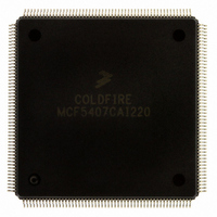
MCF5407CAI220 Freescale Semiconductor, MCF5407CAI220 Datasheet - Page 205

MCF5407CAI220
Manufacturer Part Number
MCF5407CAI220
Description
IC MPU 32B 220MHZ COLDF 208-FQFP
Manufacturer
Freescale Semiconductor
Series
MCF540xr
Specifications of MCF5407CAI220
Core Processor
Coldfire V4
Core Size
32-Bit
Speed
220MHz
Connectivity
EBI/EMI, I²C, UART/USART
Peripherals
DMA, WDT
Number Of I /o
16
Program Memory Type
ROMless
Ram Size
4K x 8
Voltage - Supply (vcc/vdd)
1.65 V ~ 3.6 V
Oscillator Type
External
Operating Temperature
-40°C ~ 85°C
Package / Case
208-FQFP
Processor Series
MCF540x
Core
ColdFire V4
Data Bus Width
32 bit
Program Memory Size
8 KB
Data Ram Size
4 KB
Maximum Clock Frequency
162 MHz
Number Of Programmable I/os
16
Operating Supply Voltage
1.8 V to 3.3 V
Mounting Style
SMD/SMT
3rd Party Development Tools
JLINK-CF-BDM26, EWCF
Cpu Speed
220MHz
Embedded Interface Type
I2C, UART
Digital Ic Case Style
FQFP
No. Of Pins
208
Supply Voltage Range
3.3V
Rohs Compliant
Yes
For Use With
M5407C3 - KIT EVAL FOR MCF5407 W/ETHERNET
Lead Free Status / RoHS Status
Lead free / RoHS Compliant
Eeprom Size
-
Program Memory Size
-
Data Converters
-
Lead Free Status / Rohs Status
Lead free / RoHS Compliant
Available stocks
Company
Part Number
Manufacturer
Quantity
Price
Company:
Part Number:
MCF5407CAI220
Manufacturer:
Freescale
Quantity:
789
Company:
Part Number:
MCF5407CAI220
Manufacturer:
Freescale Semiconductor
Quantity:
10 000
- Current page: 205 of 546
- Download datasheet (7Mb)
Breakpoint registers must be carefully configured in a development system if the processor
is executing. The debug module contains no hardware interlocks, so TDR and XTDR
should be disabled while breakpoint registers are loaded, after which TDR and XTDR can
be written to define the exact trigger. This prevents spurious breakpoint triggers.
Because there are no hardware interlocks in the debug unit, no BDM operations are allowed
while the CPU is writing the debug’s registers (DSCLK must be inactive).
5.7 Motorola-Recommended BDM Pinout
The ColdFire BDM connector, Figure 5-46, is a 26-pin Berg connector arranged 2 x 13.
5.8 Debug C Definition of PSTDDATA Outputs
This section specifies the ColdFire processor and debug module’s generation of the
PSTDDATA output on an instruction basis. In general, the PSTDDATA output for an
instruction is defined as PSTDDATA = 1, {[89B], operand} where the {...} definition is
optional operand information defined by the setting of the CSR. The [89B] signifies a PST
value that is a marker identifying the presence and size of valid data to follow. A PST value
of 0x8 (1 byte of data), 0x9 (2 bytes), or 0xB (4 bytes) is displayed before the data output.
The CSR allows operands to be displayed based on reference type (read, write, or both). A
PST value {0x8, 0x9, or 0xB} identifies the size and presence of valid data to follow on the
PSTDDATA output {1, 2, or 4 bytes}. Additionally, for certain change-of-flow branch
instructions, CSR[9,8] provides the ability to display {0x2, 0x3, or 0x4} bytes of the target
instruction address. A PST value {0x9, 0xA, or 0xB} provides the marker identifying the
size and presence of a valid target address on the PSTDDATA output.
Developer reserved
1
2
Motorola reserved
Pins reserved for BDM developer use.
Supplied by target.
PSTDDATA6
PSTDDATA4
PSTDDATA2
PSTDDATA0
VDD_CPU
RESET
+3.3V
GND
GND
GND
GND
Figure 5-46. Recommended BDM Connector
1
2
Chapter 5. Debug Support
1
3
5
7
9
11
13
15
17
19
21
23
25
10
12
14
16
18
20
22
24
26
2
4
6
8
Motorola-Recommended BDM Pinout
BKPT
DSCLK
Developer reserved
DSI
DSO
PSTDDATA7
PSTDDATA5
PSTDDATA3
PSTDDATA1
GND
Motorola reserved
PSTCLK
TA
1
5-49
Related parts for MCF5407CAI220
Image
Part Number
Description
Manufacturer
Datasheet
Request
R
Part Number:
Description:
Mcf5407 Coldfire Integrated Microprocessor User
Manufacturer:
Freescale Semiconductor, Inc
Datasheet:
Part Number:
Description:
Manufacturer:
Freescale Semiconductor, Inc
Datasheet:
Part Number:
Description:
Manufacturer:
Freescale Semiconductor, Inc
Datasheet:
Part Number:
Description:
Manufacturer:
Freescale Semiconductor, Inc
Datasheet:
Part Number:
Description:
Manufacturer:
Freescale Semiconductor, Inc
Datasheet:
Part Number:
Description:
Manufacturer:
Freescale Semiconductor, Inc
Datasheet:
Part Number:
Description:
Manufacturer:
Freescale Semiconductor, Inc
Datasheet:
Part Number:
Description:
Manufacturer:
Freescale Semiconductor, Inc
Datasheet:
Part Number:
Description:
Manufacturer:
Freescale Semiconductor, Inc
Datasheet:
Part Number:
Description:
Manufacturer:
Freescale Semiconductor, Inc
Datasheet:
Part Number:
Description:
Manufacturer:
Freescale Semiconductor, Inc
Datasheet:
Part Number:
Description:
Manufacturer:
Freescale Semiconductor, Inc
Datasheet:
Part Number:
Description:
Manufacturer:
Freescale Semiconductor, Inc
Datasheet:
Part Number:
Description:
Manufacturer:
Freescale Semiconductor, Inc
Datasheet:
Part Number:
Description:
Manufacturer:
Freescale Semiconductor, Inc
Datasheet:


