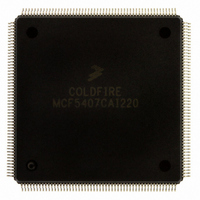
MCF5407CAI220 Freescale Semiconductor, MCF5407CAI220 Datasheet - Page 259

MCF5407CAI220
Manufacturer Part Number
MCF5407CAI220
Description
IC MPU 32B 220MHZ COLDF 208-FQFP
Manufacturer
Freescale Semiconductor
Series
MCF540xr
Specifications of MCF5407CAI220
Core Processor
Coldfire V4
Core Size
32-Bit
Speed
220MHz
Connectivity
EBI/EMI, I²C, UART/USART
Peripherals
DMA, WDT
Number Of I /o
16
Program Memory Type
ROMless
Ram Size
4K x 8
Voltage - Supply (vcc/vdd)
1.65 V ~ 3.6 V
Oscillator Type
External
Operating Temperature
-40°C ~ 85°C
Package / Case
208-FQFP
Processor Series
MCF540x
Core
ColdFire V4
Data Bus Width
32 bit
Program Memory Size
8 KB
Data Ram Size
4 KB
Maximum Clock Frequency
162 MHz
Number Of Programmable I/os
16
Operating Supply Voltage
1.8 V to 3.3 V
Mounting Style
SMD/SMT
3rd Party Development Tools
JLINK-CF-BDM26, EWCF
Cpu Speed
220MHz
Embedded Interface Type
I2C, UART
Digital Ic Case Style
FQFP
No. Of Pins
208
Supply Voltage Range
3.3V
Rohs Compliant
Yes
For Use With
M5407C3 - KIT EVAL FOR MCF5407 W/ETHERNET
Lead Free Status / RoHS Status
Lead free / RoHS Compliant
Eeprom Size
-
Program Memory Size
-
Data Converters
-
Lead Free Status / Rohs Status
Lead free / RoHS Compliant
Available stocks
Company
Part Number
Manufacturer
Quantity
Price
Company:
Part Number:
MCF5407CAI220
Manufacturer:
Freescale
Quantity:
789
Company:
Part Number:
MCF5407CAI220
Manufacturer:
Freescale Semiconductor
Quantity:
10 000
- Current page: 259 of 546
- Download datasheet (7Mb)
Chapter 10
Chip-Select Module
This chapter describes the MCF5407 chip-select module, including the operation and
programming model of the chip-select registers, which include the chip-select address,
mask, and control registers.
10.1 Overview
The following list summarizes the key chip-select features:
10.2 Chip-Select Module Signals
Table 10-1 lists signals used by the chip-select module.
Table 10-2 shows the interaction of the byte enable/byte-write enables with related signals.
Chip Selects
(CS[7:0])
Output
Enable (OE)
Byte Enables/
Byte Write
Enables
(BE[3:0]/
BWE[3:0])
• Eight independent, user-programmable chip-select signals (CS[7:0]) that can
• Address masking for 64-Kbyte to 4-Gbyte memory block sizes
• Programmable wait states and port sizes
• External master access to chip selects
Signal
interface with SRAM, PROM, EPROM, EEPROM, Flash, and peripherals
Each CSn can be independently programmed for an address location as well as for masking, port
size, read/write burst-capability, wait-state generation, and internal/external termination. Only CS0
is initialized at reset when it acts as a global chip select that allows boot ROM to be at any defined
address space. Port size and termination (internal versus external) and byte enables for CS0 are
configured by the logic levels of D[7:5] when RSTI negates.
Interfaces to memory or to peripheral devices and enables a read transfer. It is asserted and
negated on the falling edge of the clock. OE is asserted only when one of the chip selects matches
for the current address decode.
These multiplexed signals are individually programmed through the byte enable mode bit,
CSCRn[BEM], described in Section 10.4.1.3, “Chip-Select Control Registers (CSCR0–CSCR7).”
These generated signals provide byte data select signals, which are decoded from the transfer
size, A1, and A0 signals in addition to the programmed port size and burstability of the memory
accessed, as Table 10-2 shows.
Table 10-1. Chip-Select Module Signals
Chapter 10. Chip-Select Module
Description
10-1
Related parts for MCF5407CAI220
Image
Part Number
Description
Manufacturer
Datasheet
Request
R
Part Number:
Description:
Mcf5407 Coldfire Integrated Microprocessor User
Manufacturer:
Freescale Semiconductor, Inc
Datasheet:
Part Number:
Description:
Manufacturer:
Freescale Semiconductor, Inc
Datasheet:
Part Number:
Description:
Manufacturer:
Freescale Semiconductor, Inc
Datasheet:
Part Number:
Description:
Manufacturer:
Freescale Semiconductor, Inc
Datasheet:
Part Number:
Description:
Manufacturer:
Freescale Semiconductor, Inc
Datasheet:
Part Number:
Description:
Manufacturer:
Freescale Semiconductor, Inc
Datasheet:
Part Number:
Description:
Manufacturer:
Freescale Semiconductor, Inc
Datasheet:
Part Number:
Description:
Manufacturer:
Freescale Semiconductor, Inc
Datasheet:
Part Number:
Description:
Manufacturer:
Freescale Semiconductor, Inc
Datasheet:
Part Number:
Description:
Manufacturer:
Freescale Semiconductor, Inc
Datasheet:
Part Number:
Description:
Manufacturer:
Freescale Semiconductor, Inc
Datasheet:
Part Number:
Description:
Manufacturer:
Freescale Semiconductor, Inc
Datasheet:
Part Number:
Description:
Manufacturer:
Freescale Semiconductor, Inc
Datasheet:
Part Number:
Description:
Manufacturer:
Freescale Semiconductor, Inc
Datasheet:
Part Number:
Description:
Manufacturer:
Freescale Semiconductor, Inc
Datasheet:


