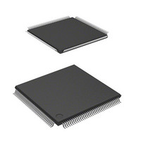
DF2166VT33WV Renesas Electronics America, DF2166VT33WV Datasheet - Page 509

DF2166VT33WV
Manufacturer Part Number
DF2166VT33WV
Description
MCU 16BIT FLASH 3V 512K 144-TQFP
Manufacturer
Renesas Electronics America
Series
H8® H8S/2100r
Datasheet
1.HS2168EPI61H-U.pdf
(876 pages)
Specifications of DF2166VT33WV
Core Processor
H8S/2000
Core Size
16-Bit
Speed
33MHz
Connectivity
I²C, IrDA, LPC, SCI, SmartCard
Peripherals
POR, PWM, WDT
Number Of I /o
106
Program Memory Size
512KB (512K x 8)
Program Memory Type
FLASH
Ram Size
40K x 8
Voltage - Supply (vcc/vdd)
3 V ~ 3.6 V
Data Converters
A/D 8x10b; D/A 2x8b
Oscillator Type
External
Operating Temperature
-20°C ~ 75°C
Package / Case
144-TQFP, 144-VQFP
Lead Free Status / RoHS Status
Lead free / RoHS Compliant
Eeprom Size
-
Available stocks
Company
Part Number
Manufacturer
Quantity
Price
Company:
Part Number:
DF2166VT33WV
Manufacturer:
Renesas Electronics America
Quantity:
135
Company:
Part Number:
DF2166VT33WV
Manufacturer:
Renesas Electronics America
Quantity:
10 000
- Current page: 509 of 876
- Download datasheet (5Mb)
15.4.2
Initialize the IIC by the procedure shown in figure 15.6 before starting transmission/reception of
data.
Note: Be sure to modify the ICMR register after transmit/receive operation has been completed.
15.4.3
In I
data, and the slave device returns an acknowledge signal.
2
C bus format master transmit mode, the master device outputs the transmit clock and transmit
If the ICMR register is modified during transmit/receive operation, bit counter BC2 to
BC0 will be modified erroneously, thus causing incorrect operation.
<< Start transmit/receive operation >>
Initialization
Master Transmit Operation
MSTP2 = 0 (IIC_2, IIC_3)
MSTP0 = 0 (IIC_4, IIC_5)
Set MSTP4 = 0 (IIC_0)
Set IICE = 1 in STCR
Set STCR and IICX3
Set ICE = 0 in ICCR
Set ICE = 1 in ICCR
Set SAR and SARX
MSTP3 = 0 (IIC_1)
Start initialization
(MSTPCRL)
Set ICMR
Set ICCR
Set ICSR
Set ICXR
Figure 15.6 Sample Flowchart for IIC Initialization
Cancel module stop mode
Enable the CPU accessing to the IIC control register and data register
Enable SAR and SARX to be accessed
Set the first and second slave addresses and IIC communication format
(SVA6 to SVA0, FS, SVAX6 to SVAX0, and FSX)
Enable ICMR and ICDR to be accessed
Use SCL/SDA pin as an IIC port
Set acknowledge bit (ACKB)
Set transfer rate (IICX and TCSS)
Set communication format, wait insertion, and transfer rate
(MLS, WAIT, CKS2 to CKS0)
Enable interrupt
(STOPIM, HNDS, ALIE, ALSL, FNC1, and FNC0)
Set interrupt enable, transfer mode, and acknowledge decision
(IEIC, MST, TRS, and ACKE)
Rev. 3.00, 03/04, page 467 of 830
Related parts for DF2166VT33WV
Image
Part Number
Description
Manufacturer
Datasheet
Request
R

Part Number:
Description:
KIT STARTER FOR M16C/29
Manufacturer:
Renesas Electronics America
Datasheet:

Part Number:
Description:
KIT STARTER FOR R8C/2D
Manufacturer:
Renesas Electronics America
Datasheet:

Part Number:
Description:
R0K33062P STARTER KIT
Manufacturer:
Renesas Electronics America
Datasheet:

Part Number:
Description:
KIT STARTER FOR R8C/23 E8A
Manufacturer:
Renesas Electronics America
Datasheet:

Part Number:
Description:
KIT STARTER FOR R8C/25
Manufacturer:
Renesas Electronics America
Datasheet:

Part Number:
Description:
KIT STARTER H8S2456 SHARPE DSPLY
Manufacturer:
Renesas Electronics America
Datasheet:

Part Number:
Description:
KIT STARTER FOR R8C38C
Manufacturer:
Renesas Electronics America
Datasheet:

Part Number:
Description:
KIT STARTER FOR R8C35C
Manufacturer:
Renesas Electronics America
Datasheet:

Part Number:
Description:
KIT STARTER FOR R8CL3AC+LCD APPS
Manufacturer:
Renesas Electronics America
Datasheet:

Part Number:
Description:
KIT STARTER FOR RX610
Manufacturer:
Renesas Electronics America
Datasheet:

Part Number:
Description:
KIT STARTER FOR R32C/118
Manufacturer:
Renesas Electronics America
Datasheet:

Part Number:
Description:
KIT DEV RSK-R8C/26-29
Manufacturer:
Renesas Electronics America
Datasheet:

Part Number:
Description:
KIT STARTER FOR SH7124
Manufacturer:
Renesas Electronics America
Datasheet:

Part Number:
Description:
KIT STARTER FOR H8SX/1622
Manufacturer:
Renesas Electronics America
Datasheet:

Part Number:
Description:
KIT DEV FOR SH7203
Manufacturer:
Renesas Electronics America
Datasheet:


