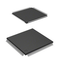
DF2166VT33WV Renesas Electronics America, DF2166VT33WV Datasheet - Page 51

DF2166VT33WV
Manufacturer Part Number
DF2166VT33WV
Description
MCU 16BIT FLASH 3V 512K 144-TQFP
Manufacturer
Renesas Electronics America
Series
H8® H8S/2100r
Datasheet
1.HS2168EPI61H-U.pdf
(876 pages)
Specifications of DF2166VT33WV
Core Processor
H8S/2000
Core Size
16-Bit
Speed
33MHz
Connectivity
I²C, IrDA, LPC, SCI, SmartCard
Peripherals
POR, PWM, WDT
Number Of I /o
106
Program Memory Size
512KB (512K x 8)
Program Memory Type
FLASH
Ram Size
40K x 8
Voltage - Supply (vcc/vdd)
3 V ~ 3.6 V
Data Converters
A/D 8x10b; D/A 2x8b
Oscillator Type
External
Operating Temperature
-20°C ~ 75°C
Package / Case
144-TQFP, 144-VQFP
Lead Free Status / RoHS Status
Lead free / RoHS Compliant
Eeprom Size
-
Available stocks
Company
Part Number
Manufacturer
Quantity
Price
Company:
Part Number:
DF2166VT33WV
Manufacturer:
Renesas Electronics America
Quantity:
135
Company:
Part Number:
DF2166VT33WV
Manufacturer:
Renesas Electronics America
Quantity:
10 000
- Current page: 51 of 876
- Download datasheet (5Mb)
1.3.3
Table 1.2
Type
Power
supply
Clock
Operating
mode
control
System
control
Address
bus
Data bus
Pin Functions
Pin Functions
VCC
VCL
VSS
XTAL
EXTAL
φ
EXCL
PFSEL
MD2
MD1
MD0
RES
RESO
STBY
FWE
A23 to A16 33 to 35
A15 to A0
D15 to D8 128 to 121 Input/
D7 to D0
Symbol
Pin No.
1, 36
86
13
7, 42,
95, 111
139
143
144
18
18
141
14
9
10
8
142
12
135
37 to 41
96 to 110
112
85 to 78
I/O
Input
Input
Input
Input
Input
Output
Input
Input
Input
Input
Output
Input
Input
Output
Output
Name and Function
Power supply pins. Connect all these pins to the
system power supply. Connect the bypass
capacitor between VCC and VSS (near VCC).
External capacitance pin for internal step-down
power. Connect this pin to Vss through an
external capacitor (that is located near this pin) to
stabilize internal step-down power.
Ground pins. Connect all these pins to the system
power supply (0V).
For connection to a crystal resonator. An external
clock can be supplied from the EXTAL pin. For an
example of crystal resonator connection, see
section 22, Clock Pulse Generator.
Supplies the system clock to external devices.
32.768-kHz external clock for sub clock should be
supplied.
Pin for use by PLL. For an example of PLL
connection, see section 22, Clock Pulse
Generator.
These pins set the operating mode. Inputs at
these pins should not be changed during
operation.
Reset pin. When this pin is low, the chip is reset.
Outputs a reset signal to an external device.
When this pin is low, a transition is made to
hardware standby mode.
Pin for use by flash memory.
Address output pins
Upper bidirectional data bus
Lower bidirectional data bus
Rev. 3.00, 03/04, page 9 of 830
Related parts for DF2166VT33WV
Image
Part Number
Description
Manufacturer
Datasheet
Request
R

Part Number:
Description:
KIT STARTER FOR M16C/29
Manufacturer:
Renesas Electronics America
Datasheet:

Part Number:
Description:
KIT STARTER FOR R8C/2D
Manufacturer:
Renesas Electronics America
Datasheet:

Part Number:
Description:
R0K33062P STARTER KIT
Manufacturer:
Renesas Electronics America
Datasheet:

Part Number:
Description:
KIT STARTER FOR R8C/23 E8A
Manufacturer:
Renesas Electronics America
Datasheet:

Part Number:
Description:
KIT STARTER FOR R8C/25
Manufacturer:
Renesas Electronics America
Datasheet:

Part Number:
Description:
KIT STARTER H8S2456 SHARPE DSPLY
Manufacturer:
Renesas Electronics America
Datasheet:

Part Number:
Description:
KIT STARTER FOR R8C38C
Manufacturer:
Renesas Electronics America
Datasheet:

Part Number:
Description:
KIT STARTER FOR R8C35C
Manufacturer:
Renesas Electronics America
Datasheet:

Part Number:
Description:
KIT STARTER FOR R8CL3AC+LCD APPS
Manufacturer:
Renesas Electronics America
Datasheet:

Part Number:
Description:
KIT STARTER FOR RX610
Manufacturer:
Renesas Electronics America
Datasheet:

Part Number:
Description:
KIT STARTER FOR R32C/118
Manufacturer:
Renesas Electronics America
Datasheet:

Part Number:
Description:
KIT DEV RSK-R8C/26-29
Manufacturer:
Renesas Electronics America
Datasheet:

Part Number:
Description:
KIT STARTER FOR SH7124
Manufacturer:
Renesas Electronics America
Datasheet:

Part Number:
Description:
KIT STARTER FOR H8SX/1622
Manufacturer:
Renesas Electronics America
Datasheet:

Part Number:
Description:
KIT DEV FOR SH7203
Manufacturer:
Renesas Electronics America
Datasheet:


