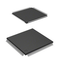
DF2166VT33WV Renesas Electronics America, DF2166VT33WV Datasheet - Page 760

DF2166VT33WV
Manufacturer Part Number
DF2166VT33WV
Description
MCU 16BIT FLASH 3V 512K 144-TQFP
Manufacturer
Renesas Electronics America
Series
H8® H8S/2100r
Datasheet
1.HS2168EPI61H-U.pdf
(876 pages)
Specifications of DF2166VT33WV
Core Processor
H8S/2000
Core Size
16-Bit
Speed
33MHz
Connectivity
I²C, IrDA, LPC, SCI, SmartCard
Peripherals
POR, PWM, WDT
Number Of I /o
106
Program Memory Size
512KB (512K x 8)
Program Memory Type
FLASH
Ram Size
40K x 8
Voltage - Supply (vcc/vdd)
3 V ~ 3.6 V
Data Converters
A/D 8x10b; D/A 2x8b
Oscillator Type
External
Operating Temperature
-20°C ~ 75°C
Package / Case
144-TQFP, 144-VQFP
Lead Free Status / RoHS Status
Lead free / RoHS Compliant
Eeprom Size
-
Available stocks
Company
Part Number
Manufacturer
Quantity
Price
Company:
Part Number:
DF2166VT33WV
Manufacturer:
Renesas Electronics America
Quantity:
135
Company:
Part Number:
DF2166VT33WV
Manufacturer:
Renesas Electronics America
Quantity:
10 000
- Current page: 760 of 876
- Download datasheet (5Mb)
21.6
1. A reset must always be executed by driving the ETRST pin to 0, regardless of whether or not
2. The following must be considered when the power-on reset signal is applied to the ETRST pin.
3. The registers are not initialized in standby mode. If the ETRST pin is set to 0 in standby mode,
4. The frequency of the ETCK pin must be lower than that of the system clock. For details, see
5. Data input/output in serial data transfer starts from the LSB. Figure 21.4 and 21.5 shows
6. When data that exceeds the number of bits of the register connected between the ETDI and
7. If the JTAG serial transfer sequence is disrupted, the ETRST pin must be reset. Transfer
8. If a pin with a pull-up function is sampled while its pull-up function is enabled, 1 can be
Rev. 3.00, 03/04, page 718 of 830
the JTAG is to be activated. The ETRST pin must be held low for 20 ETCK clock cycles. For
details, see section 25, Electrical Characteristics. To activate the JTAG after a reset, drive the
ETRST pin to 1 and specify the ETCK, ETMS, and ETDI pins to any value. If the JTAG is not
to be activated, drive the ETRST, ETCK, ETMS, and ETDI pins to 1 or the high-impedance
state. These pins are internally pulled up and are noted in standby mode.
The reset signal must be applied at power-on.
To prevent the LSI system operation from being affected by the ETRST pin of the board
Alternatively, to prevent the ETRST pin of the board tester from being affected by the LSI
Figure 21.3 shows a design example of the reset signal circuit wherein no reset signal
interference occurs.
IDCODE mode will be entered.
section 25, Electrical Characteristics.
examples of serial data input/output.
ETDO pins is serially transferred, the serial data that exceeds the number of register bits and
output from the ETDO pin is the same as that input from the ETDI pin.
should then be retried, regardless of the transfer operation.
detected at the corresponding input scan register. In this case, the corresponding enable scan
register should be cleared to 0.
tester, circuits must be separated .
system reset, circuits must be separated.
Usage Notes
System reset
Figure 21.3 Reset Signal Circuit Without Reset Signal Interference
ETRST
Board edge pin
Power-on
reset circuit
RES
ETRST
This LSI
Related parts for DF2166VT33WV
Image
Part Number
Description
Manufacturer
Datasheet
Request
R

Part Number:
Description:
KIT STARTER FOR M16C/29
Manufacturer:
Renesas Electronics America
Datasheet:

Part Number:
Description:
KIT STARTER FOR R8C/2D
Manufacturer:
Renesas Electronics America
Datasheet:

Part Number:
Description:
R0K33062P STARTER KIT
Manufacturer:
Renesas Electronics America
Datasheet:

Part Number:
Description:
KIT STARTER FOR R8C/23 E8A
Manufacturer:
Renesas Electronics America
Datasheet:

Part Number:
Description:
KIT STARTER FOR R8C/25
Manufacturer:
Renesas Electronics America
Datasheet:

Part Number:
Description:
KIT STARTER H8S2456 SHARPE DSPLY
Manufacturer:
Renesas Electronics America
Datasheet:

Part Number:
Description:
KIT STARTER FOR R8C38C
Manufacturer:
Renesas Electronics America
Datasheet:

Part Number:
Description:
KIT STARTER FOR R8C35C
Manufacturer:
Renesas Electronics America
Datasheet:

Part Number:
Description:
KIT STARTER FOR R8CL3AC+LCD APPS
Manufacturer:
Renesas Electronics America
Datasheet:

Part Number:
Description:
KIT STARTER FOR RX610
Manufacturer:
Renesas Electronics America
Datasheet:

Part Number:
Description:
KIT STARTER FOR R32C/118
Manufacturer:
Renesas Electronics America
Datasheet:

Part Number:
Description:
KIT DEV RSK-R8C/26-29
Manufacturer:
Renesas Electronics America
Datasheet:

Part Number:
Description:
KIT STARTER FOR SH7124
Manufacturer:
Renesas Electronics America
Datasheet:

Part Number:
Description:
KIT STARTER FOR H8SX/1622
Manufacturer:
Renesas Electronics America
Datasheet:

Part Number:
Description:
KIT DEV FOR SH7203
Manufacturer:
Renesas Electronics America
Datasheet:


