MC68302EH16C Freescale Semiconductor, MC68302EH16C Datasheet - Page 18
MC68302EH16C
Manufacturer Part Number
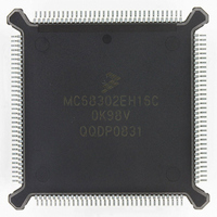
MC68302EH16C
Description
IC MPU MULTI-PROTOCOL 132-PQFP
Manufacturer
Freescale Semiconductor
Datasheets
1.MC68302AG20C.pdf
(4 pages)
2.MC68302AG20C.pdf
(2 pages)
3.MC68302AG20C.pdf
(13 pages)
4.MC68302EH16C.pdf
(481 pages)
Specifications of MC68302EH16C
Processor Type
M683xx 32-Bit
Speed
16MHz
Voltage
5V
Mounting Type
Surface Mount
Package / Case
132-MQFP, 132-PQFP
Controller Family/series
68K
Core Size
32 Bit
Ram Memory Size
1152Byte
Cpu Speed
16MHz
No. Of Timers
3
Embedded Interface Type
SCP, TDM
Digital Ic Case Style
PQFP
Rohs Compliant
Yes
Family Name
M68000
Device Core
ColdFire
Device Core Size
32b
Frequency (max)
16MHz
Instruction Set Architecture
RISC
Supply Voltage 1 (typ)
5V
Operating Temp Range
0C to 70C
Operating Temperature Classification
Commercial
Mounting
Surface Mount
Pin Count
132
Package Type
PQFP
Lead Free Status / RoHS Status
Lead free / RoHS Compliant
Features
-
Lead Free Status / Rohs Status
RoHS Compliant part
Electrostatic Device
Available stocks
Company
Part Number
Manufacturer
Quantity
Price
Company:

Part Number:
MC68302EH16C
Manufacturer:
Freescale Semiconductor
Quantity:
135
Company:
Part Number:
MC68302EH16C
Manufacturer:
PANA
Quantity:
99
Company:
Part Number:
MC68302EH16C
Manufacturer:
Freescale Semiconductor
Quantity:
10 000
Part Number:
MC68302EH16C
Manufacturer:
FREESCALE
Quantity:
20 000
Company:
Part Number:
MC68302EH16CB1
Manufacturer:
Freescale Semiconductor
Quantity:
10 000
Company:
Part Number:
MC68302EH16CR2
Manufacturer:
Freescale Semiconductor
Quantity:
10 000


Table of Contents
Figure
Number
Figure 4-5.
Figure 4-6.
Figure 4-7.
Figure 4-8.
Figure 4-9.
Figure 4-10. PCM Channel Assignment on a T1/CEPT Line ....................................... 4-19
Figure 4-11. SCC Block Diagram ................................................................................. 4-24
Figure 4-12. SCC Baud Rate Generator ...................................................................... 4-26
Figure 4-13. Output Delays from RTS Low, Synchronous Protocol ............................. 4-29
Figure 4-14. Output Delays from CTS Low, Synchronous Protocol ............................. 4-29
Figure 4-15. Memory Structure..................................................................................... 4-32
Figure 4-16. SCC Buffer Descriptor Format ................................................................. 4-33
Figure 4-17. UART Frame Format................................................................................ 4-43
Figure 4-18. Two Configurations of UART Multidrop Operation................................... 4-50
Figure 4-19. UART Control Characters Table .............................................................. 4-51
Figure 4-20. UART Receive Buffer Descriptor ............................................................. 4-58
Figure 4-21. UART Rx BD Example ............................................................................. 4-59
Figure 4-22. UART Transmit Buffer Descriptor ............................................................ 4-61
Figure 4-23. UART Interrupt Events Example .............................................................. 4-64
Figure 4-24. Typical HDLC Frame................................................................................ 4-66
Figure 4-25. HDLC Address Recognition Examples .................................................... 4-71
Figure 4-26. HDLC Receive Buffer Descriptor ............................................................. 4-75
Figure 4-27. HDLC Receive BD Example .................................................................... 4-76
Figure 4-28. HDLC Transmit Buffer Descriptor ............................................................ 4-78
Figure 4-29. HDLC Interrupt Events Example .............................................................. 4-81
Figure 4-30. Typical BISYNC Frames .......................................................................... 4-83
Figure 4-31. BISYNC Control Characters Table........................................................... 4-88
Figure 4-32. BISYNC Receive Buffer Descriptor.......................................................... 4-93
Figure 4-33. BISYNC Transmit Buffer Descriptor......................................................... 4-95
Figure 4-34. Typical DDCMP Frames ........................................................................ 4-100
Figure 4-35. DDCMP Transmission/Reception Summary .......................................... 4-102
Figure 4-36. DDCMP Receive Buffer Descriptor ........................................................ 4-109
Figure 4-37. DDCMP Transmit Buffer Descriptor ....................................................... 4-112
Figure 4-38. Two-Step Synchronous Bit Rate Adaption............................................. 4-116
Figure 4-39. Three-Step Asynchronous Bit Rate Adaption ........................................ 4-117
Figure 4-40. V.110 Receive Buffer Descriptor............................................................ 4-119
Figure 4-41. V.110 Transmit Buffer Descriptor........................................................... 4-120
Figure 4-42. Transparent Receive Buffer Descriptor.................................................. 4-130
Figure 4-43. Transparent Transmit Buffer Descriptor................................................. 4-131
Figure 4-44. SCP Timing ............................................................................................ 4-135
Figure 4-45. SCP vs. SCC Pin Multiplexing ............................................................... 4-137
Figure 5-1.
xviii
Serial Channels Physical Interface Block Diagram .................................. 4-10
IDL Bus Signals ....................................................................................... 4-11
IDL Terminal Adaptor ............................................................................... 4-12
GCI Bus Signals....................................................................................... 4-15
Two PCM Sync Methods.......................................................................... 4-18
Functional Signal Groups........................................................................... 5-3
MC68302 USER’S MANUAL
Signal Description
Section 5
Title
MOTOROLA
Number
Page
Related parts for MC68302EH16C
Image
Part Number
Description
Manufacturer
Datasheet
Request
R

Part Number:
Description:
Manufacturer:
Freescale Semiconductor, Inc
Datasheet:

Part Number:
Description:
MC68302 Configuring the Chip Selects on the MC68302
Manufacturer:
Motorola / Freescale Semiconductor
Part Number:
Description:
MC68302 Design Concept - Expanding Interrupts on the MC68302
Manufacturer:
Motorola / Freescale Semiconductor
Part Number:
Description:
MC68302 MC68302 Adapting a WAN Controller to a LAN Environment
Manufacturer:
Motorola / Freescale Semiconductor
Part Number:
Description:
MC68302 EKB Applications - Power Measurements on the MC68302
Manufacturer:
Motorola / Freescale Semiconductor
Part Number:
Description:
MC68302 Interfacing the MC68020 to a Slave MC68302
Manufacturer:
Motorola / Freescale Semiconductor
Part Number:
Description:
MC68302 MC68302 Software Performance
Manufacturer:
Motorola / Freescale Semiconductor
Part Number:
Description:
MC68302 Evaluating EDX on the ADS302
Manufacturer:
Motorola / Freescale Semiconductor
Part Number:
Description:
MC68302 Design Advisory #1 - MC68SC302 Passive ISDN Protocol Engine
Manufacturer:
Motorola / Freescale Semiconductor
Part Number:
Description:
MC68302, MC68360, and MPC860 Characteristics and Design Notes for Crystal Feedback Oscillators
Manufacturer:
Motorola / Freescale Semiconductor
Part Number:
Description:
Mc68302 Integrated Multi-protocol Processor
Manufacturer:
Freescale Semiconductor, Inc
Datasheet:
Part Number:
Description:
Manufacturer:
Freescale Semiconductor, Inc
Datasheet:
Part Number:
Description:
Manufacturer:
Freescale Semiconductor, Inc
Datasheet:
Part Number:
Description:
Manufacturer:
Freescale Semiconductor, Inc
Datasheet:
Part Number:
Description:
Manufacturer:
Freescale Semiconductor, Inc
Datasheet: