MC68302EH16C Freescale Semiconductor, MC68302EH16C Datasheet - Page 97
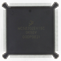
MC68302EH16C
Manufacturer Part Number
MC68302EH16C
Description
IC MPU MULTI-PROTOCOL 132-PQFP
Manufacturer
Freescale Semiconductor
Datasheets
1.MC68302AG20C.pdf
(4 pages)
2.MC68302AG20C.pdf
(2 pages)
3.MC68302AG20C.pdf
(13 pages)
4.MC68302EH16C.pdf
(481 pages)
Specifications of MC68302EH16C
Processor Type
M683xx 32-Bit
Speed
16MHz
Voltage
5V
Mounting Type
Surface Mount
Package / Case
132-MQFP, 132-PQFP
Controller Family/series
68K
Core Size
32 Bit
Ram Memory Size
1152Byte
Cpu Speed
16MHz
No. Of Timers
3
Embedded Interface Type
SCP, TDM
Digital Ic Case Style
PQFP
Rohs Compliant
Yes
Family Name
M68000
Device Core
ColdFire
Device Core Size
32b
Frequency (max)
16MHz
Instruction Set Architecture
RISC
Supply Voltage 1 (typ)
5V
Operating Temp Range
0C to 70C
Operating Temperature Classification
Commercial
Mounting
Surface Mount
Pin Count
132
Package Type
PQFP
Lead Free Status / RoHS Status
Lead free / RoHS Compliant
Features
-
Lead Free Status / Rohs Status
RoHS Compliant part
Electrostatic Device
Available stocks
Company
Part Number
Manufacturer
Quantity
Price
Company:

Part Number:
MC68302EH16C
Manufacturer:
Freescale Semiconductor
Quantity:
135
Company:
Part Number:
MC68302EH16C
Manufacturer:
PANA
Quantity:
99
Company:
Part Number:
MC68302EH16C
Manufacturer:
Freescale Semiconductor
Quantity:
10 000
Part Number:
MC68302EH16C
Manufacturer:
FREESCALE
Quantity:
20 000
Company:
Part Number:
MC68302EH16CB1
Manufacturer:
Freescale Semiconductor
Quantity:
10 000
Company:
Part Number:
MC68302EH16CR2
Manufacturer:
Freescale Semiconductor
Quantity:
10 000


EN—Enable
3.6.2.2 Option Registers (OR3–OR0)
These four 16-bit registers consist of a base address mask field, a read/write mask bit, a
compare function code bit, and a DTACK generation field.
Bits 15–12—DTACK Field
When all the bits in this field are set to one, DTACK must be generated externally, and the
IMP or external bus master waits for DTACK (input) to terminate its bus cycle. After system
reset, the bits of the DTACK field default to six wait states.
The DTACK generator uses the IMP internal clock to generate the programmable number
of wait states. For asynchronous external bus masters, the programmable number of wait
states is counted directly from the internal clock. When no wait state is programmed
(DTACK = 000), the DTACK generator will generate DTACK asynchronously.
The CS lines are asserted slightly earlier for internal IMP master memory cycles than for an
external master using the CS lines. Set external master wait state (EMWS) in the SCR
whenever these timing differences require an extra memory wait state for external masters.
MOTOROLA
After system reset, only CS0 is enabled; CS3–CS1 are disabled. In disable CPU mode,
CS3–CS0 are disabled at system reset. The chip select does not require disabling before
changing its parameters.
These bits are used to determine whether DTACK is generated internally with a program-
mable number of wait states or externally by the peripheral. With internal DTACK gener-
ation, zero to six wait states can be automatically inserted before the DTACK pin is
asserted as an output (see Port A Control Register (PACNT)).
15
0 = The chip-select line is disabled.
1 = The chip-select line is enabled.
DTACK
13
12
15
0
0
0
0
1
1
1
1
Table 3-8. DTACK Field Encoding
Bits
14
MC68302 USER’S MANUAL
0
0
1
1
0
0
1
1
BASE ADDRESS MASK (M23–M13)
13
0
1
0
1
0
1
0
1
No Wait State
1 Wait State
2 Wait States
3 Wait States
4 Wait States
5 Wait States
6 Wait States
External DTACK
Description
System Integration Block (SIB)
2
MRW
1
CFC
3-47
0
Related parts for MC68302EH16C
Image
Part Number
Description
Manufacturer
Datasheet
Request
R

Part Number:
Description:
Manufacturer:
Freescale Semiconductor, Inc
Datasheet:

Part Number:
Description:
MC68302 Configuring the Chip Selects on the MC68302
Manufacturer:
Motorola / Freescale Semiconductor
Part Number:
Description:
MC68302 Design Concept - Expanding Interrupts on the MC68302
Manufacturer:
Motorola / Freescale Semiconductor
Part Number:
Description:
MC68302 MC68302 Adapting a WAN Controller to a LAN Environment
Manufacturer:
Motorola / Freescale Semiconductor
Part Number:
Description:
MC68302 EKB Applications - Power Measurements on the MC68302
Manufacturer:
Motorola / Freescale Semiconductor
Part Number:
Description:
MC68302 Interfacing the MC68020 to a Slave MC68302
Manufacturer:
Motorola / Freescale Semiconductor
Part Number:
Description:
MC68302 MC68302 Software Performance
Manufacturer:
Motorola / Freescale Semiconductor
Part Number:
Description:
MC68302 Evaluating EDX on the ADS302
Manufacturer:
Motorola / Freescale Semiconductor
Part Number:
Description:
MC68302 Design Advisory #1 - MC68SC302 Passive ISDN Protocol Engine
Manufacturer:
Motorola / Freescale Semiconductor
Part Number:
Description:
MC68302, MC68360, and MPC860 Characteristics and Design Notes for Crystal Feedback Oscillators
Manufacturer:
Motorola / Freescale Semiconductor
Part Number:
Description:
Mc68302 Integrated Multi-protocol Processor
Manufacturer:
Freescale Semiconductor, Inc
Datasheet:
Part Number:
Description:
Manufacturer:
Freescale Semiconductor, Inc
Datasheet:
Part Number:
Description:
Manufacturer:
Freescale Semiconductor, Inc
Datasheet:
Part Number:
Description:
Manufacturer:
Freescale Semiconductor, Inc
Datasheet:
Part Number:
Description:
Manufacturer:
Freescale Semiconductor, Inc
Datasheet: