MC68302EH16C Freescale Semiconductor, MC68302EH16C Datasheet - Page 21
MC68302EH16C
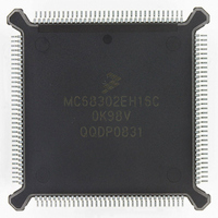
Manufacturer Part Number
MC68302EH16C
Description
IC MPU MULTI-PROTOCOL 132-PQFP
Manufacturer
Freescale Semiconductor
Datasheets
1.MC68302AG20C.pdf
(4 pages)
2.MC68302AG20C.pdf
(2 pages)
3.MC68302AG20C.pdf
(13 pages)
4.MC68302EH16C.pdf
(481 pages)
Specifications of MC68302EH16C
Processor Type
M683xx 32-Bit
Speed
16MHz
Voltage
5V
Mounting Type
Surface Mount
Package / Case
132-MQFP, 132-PQFP
Controller Family/series
68K
Core Size
32 Bit
Ram Memory Size
1152Byte
Cpu Speed
16MHz
No. Of Timers
3
Embedded Interface Type
SCP, TDM
Digital Ic Case Style
PQFP
Rohs Compliant
Yes
Family Name
M68000
Device Core
ColdFire
Device Core Size
32b
Frequency (max)
16MHz
Instruction Set Architecture
RISC
Supply Voltage 1 (typ)
5V
Operating Temp Range
0C to 70C
Operating Temperature Classification
Commercial
Mounting
Surface Mount
Pin Count
132
Package Type
PQFP
Lead Free Status / RoHS Status
Lead free / RoHS Compliant
Features
-
Lead Free Status / Rohs Status
RoHS Compliant part
Electrostatic Device
Available stocks
Company
Part Number
Manufacturer
Quantity
Price
Company:

Part Number:
MC68302EH16C
Manufacturer:
Freescale Semiconductor
Quantity:
135
Company:
Part Number:
MC68302EH16C
Manufacturer:
PANA
Quantity:
99
Company:
Part Number:
MC68302EH16C
Manufacturer:
Freescale Semiconductor
Quantity:
10 000
Part Number:
MC68302EH16C
Manufacturer:
FREESCALE
Quantity:
20 000
Company:
Part Number:
MC68302EH16CB1
Manufacturer:
Freescale Semiconductor
Quantity:
10 000
Company:
Part Number:
MC68302EH16CR2
Manufacturer:
Freescale Semiconductor
Quantity:
10 000


Table 2-1. M68000 Data Addressing Modes .................................................................2-4
Table 2-2. M68000 Instruction Set Summary.................................................................2-5
Table 2-3. M68000 Instruction Type Variations .............................................................2-6
Table 2-4. M68000 Address Spaces..............................................................................2-7
Table 2-5. M68000 Exception Vector Assignment .........................................................2-8
Table 2-6. System Configuration Register ...................................................................2-14
Table 2-7. System RAM ...............................................................................................2-14
Table 2-8. Parameter RAM ..........................................................................................2-15
Table 2-9. Internal Registers........................................................................................2-17
Table 3-1. SAPR and DAPR Incrementing Rules ........................................................3-10
Table 3-2. IDMA Bus Cycles ........................................................................................3-11
Table 3-3. EXRQ and INRQ Prioritization ....................................................................3-19
Table 3-4. INRQ Prioritization within Interrupt Level 4 .................................................3-19
Table 3-5. Encoding the Interrupt Vector .....................................................................3-23
Table 3-6. Port A Pin Functions ...................................................................................3-31
Table 3-7. Port B Pin Functions ...................................................................................3-32
Table 3-8. DTACK Field Encoding ...............................................................................3-47
Table 3-9. SCR Register Bits .......................................................................................3-51
Table 3-10. Bus Arbitration Priority Table ......................................................................3-58
Table 3-11. DRAM Refresh Memory Map Table............................................................3-68
Table 4-1. The Five Possible SCC Combinations..........................................................4-9
Table 4-2. PCM Highway Mode Pin Functions ............................................................4-17
Table 4-3. PCM Channel Selection..............................................................................4-17
Table 4-4. Typical Bit Rates of Asynchronous Communication ...................................4-27
Table 4-5. Transmit Data Delay (TCLK Periods) .........................................................4-28
Table 4-6. SCC Parameter RAM Memory Map............................................................4-35
Table 4-7. UART Specific Parameter RAM..................................................................4-46
Table 4-8. HDLC-Specific Parameter RAM..................................................................4-69
Table 4-9. BISYNC Specific Parameter RAM ..............................................................4-86
Table 4-10. DDCMP Specific Parameter RAM ............................................................4-104
Table 4-11. Transparent-Specific Parameter RAM ......................................................4-125
MOTOROLA
Table
Number
Communications Processor (CP)
System Integration Block (SIB)
LIST OF TABLES
MC68000/MC68008 Core
MC68302 USER’S MANUAL
Section 2
Section 3
Section 4
Title
Number
Page
xxi
Related parts for MC68302EH16C
Image
Part Number
Description
Manufacturer
Datasheet
Request
R

Part Number:
Description:
Manufacturer:
Freescale Semiconductor, Inc
Datasheet:

Part Number:
Description:
MC68302 Configuring the Chip Selects on the MC68302
Manufacturer:
Motorola / Freescale Semiconductor
Part Number:
Description:
MC68302 Design Concept - Expanding Interrupts on the MC68302
Manufacturer:
Motorola / Freescale Semiconductor
Part Number:
Description:
MC68302 MC68302 Adapting a WAN Controller to a LAN Environment
Manufacturer:
Motorola / Freescale Semiconductor
Part Number:
Description:
MC68302 EKB Applications - Power Measurements on the MC68302
Manufacturer:
Motorola / Freescale Semiconductor
Part Number:
Description:
MC68302 Interfacing the MC68020 to a Slave MC68302
Manufacturer:
Motorola / Freescale Semiconductor
Part Number:
Description:
MC68302 MC68302 Software Performance
Manufacturer:
Motorola / Freescale Semiconductor
Part Number:
Description:
MC68302 Evaluating EDX on the ADS302
Manufacturer:
Motorola / Freescale Semiconductor
Part Number:
Description:
MC68302 Design Advisory #1 - MC68SC302 Passive ISDN Protocol Engine
Manufacturer:
Motorola / Freescale Semiconductor
Part Number:
Description:
MC68302, MC68360, and MPC860 Characteristics and Design Notes for Crystal Feedback Oscillators
Manufacturer:
Motorola / Freescale Semiconductor
Part Number:
Description:
Mc68302 Integrated Multi-protocol Processor
Manufacturer:
Freescale Semiconductor, Inc
Datasheet:
Part Number:
Description:
Manufacturer:
Freescale Semiconductor, Inc
Datasheet:
Part Number:
Description:
Manufacturer:
Freescale Semiconductor, Inc
Datasheet:
Part Number:
Description:
Manufacturer:
Freescale Semiconductor, Inc
Datasheet:
Part Number:
Description:
Manufacturer:
Freescale Semiconductor, Inc
Datasheet: