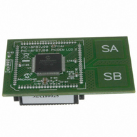
MA180025 Microchip Technology, MA180025 Datasheet - Page 128

MA180025
Manufacturer Part Number
MA180025
Description
MODULE PLUG-IN PIC18F87J90 PIM
Manufacturer
Microchip Technology
Series
PIC®r
Specifications of MA180025
Accessory Type
Plug-In Module (PIM) - PIC18F87J90
Product
Microcontroller Modules
Silicon Manufacturer
Microchip
Core Architecture
PIC
Core Sub-architecture
PIC18
Silicon Core Number
PIC18F
Silicon Family Name
PIC18FxxJxx
Lead Free Status / RoHS Status
Lead free / RoHS Compliant
For Use With/related Products
PICDEM LCD 2 Demonstration Board (DM163030)
For Use With
DM163030 - KIT DEV PICDEM LCD2
Lead Free Status / Rohs Status
Lead free / RoHS Compliant
Available stocks
Company
Part Number
Manufacturer
Quantity
Price
Company:
Part Number:
MA180025
Manufacturer:
Microchip Technology
Quantity:
135
Company:
Part Number:
MA180025
Manufacturer:
MICROCHIP
Quantity:
12 000
- Current page: 128 of 450
- Download datasheet (4Mb)
corresponding Data Direction and Output Latch registers
PIC18F87J90 FAMILY
10.6
PORTE is a 7-bit wide, bidirectional port. The
are TRISE and LATE. All pins on PORTE are digital only
and tolerate voltages up to 5.5V.
All pins on PORTE are implemented with Schmitt
Trigger input buffers. Each pin is individually
configurable as an input or output. The RE7 pin is also
configurable for open-drain output when CCP2 is active
on this pin. Open-drain configuration is selected by
setting the CCP2OD control bit (TRISG<6>)
Each of the PORTE pins has a weak internal pull-up. A
single control bit can turn off all the pull-ups. This is
performed by clearing bit, REPU (PORTG<6>). The
weak pull-up is automatically turned off when the port
pin is configured as an output. The pull-ups are
disabled on any device Reset.
Pins, RE<6:3>, are multiplexed with the LCD common
drives. I/O port functions are only available on those
PORTE pins depending on which commons are active.
The configuration is determined by the LMUX<1:0>
control bits (LCDCON<1:0>). The availability is
summarized in Table 10-11.
TABLE 10-11: PORTE PINS AVAILABLE IN
DS39933D-page 128
LCDCON
Note:
<1:0>
00
01
10
11
PORTE, TRISE and
LATE Registers
These pins are configured as digital inputs
on any device Reset.
through COM3)
COM0, COM1
COM0, COM1
Active LCD
Commons
and COM2
All (COM0
DIFFERENT LCD DRIVE
CONFIGURATIONS
COM0
PORTE Available
RE6, RE5, RE4
RE6, RE5
for I/O
None
RE6
Pins, RE1 and RE0, are multiplexed with the functions
of LCDBIAS2 and LCDBIAS1. When LCD bias genera-
tion is required (i.e., any application where the device
is connected to an external LCD), these pins cannot be
used as digital I/O.
RE7 is multiplexed with the LCD segment drive
(SEG31) controlled by the LCDSE3<7> bit. I/O port
function is only available when the segment is disabled.
RE7 can also be configured as the alternate peripheral
pin for the CCP2 module. This is done by clearing the
CCP2MX Configuration bit.
EXAMPLE 10-5:
CLRF
CLRF
MOVLW
MOVWF
Note:
PORTE
LATE
03h
TRISE
The pin corresponding to RE2 of other
PIC18F
LCDBIAS3 in this device. It cannot be used
as digital I/O.
; Initialize PORTE by
; clearing output
; data latches
; Alternate method
; to clear output
; data latches
; Value used to
; initialize data
; direction
; Set RE<1:0> as inputs
; RE<7:2> as outputs
parts
INITIALIZING PORTE
2010 Microchip Technology Inc.
has
the
function
of
Related parts for MA180025
Image
Part Number
Description
Manufacturer
Datasheet
Request
R

Part Number:
Description:
Manufacturer:
Microchip Technology Inc.
Datasheet:

Part Number:
Description:
Manufacturer:
Microchip Technology Inc.
Datasheet:

Part Number:
Description:
Manufacturer:
Microchip Technology Inc.
Datasheet:

Part Number:
Description:
Manufacturer:
Microchip Technology Inc.
Datasheet:

Part Number:
Description:
Manufacturer:
Microchip Technology Inc.
Datasheet:

Part Number:
Description:
Manufacturer:
Microchip Technology Inc.
Datasheet:

Part Number:
Description:
Manufacturer:
Microchip Technology Inc.
Datasheet:

Part Number:
Description:
Manufacturer:
Microchip Technology Inc.
Datasheet:


