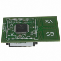
MA180025 Microchip Technology, MA180025 Datasheet - Page 174

MA180025
Manufacturer Part Number
MA180025
Description
MODULE PLUG-IN PIC18F87J90 PIM
Manufacturer
Microchip Technology
Series
PIC®r
Specifications of MA180025
Accessory Type
Plug-In Module (PIM) - PIC18F87J90
Product
Microcontroller Modules
Silicon Manufacturer
Microchip
Core Architecture
PIC
Core Sub-architecture
PIC18
Silicon Core Number
PIC18F
Silicon Family Name
PIC18FxxJxx
Lead Free Status / RoHS Status
Lead free / RoHS Compliant
For Use With/related Products
PICDEM LCD 2 Demonstration Board (DM163030)
For Use With
DM163030 - KIT DEV PICDEM LCD2
Lead Free Status / Rohs Status
Lead free / RoHS Compliant
Available stocks
Company
Part Number
Manufacturer
Quantity
Price
Company:
Part Number:
MA180025
Manufacturer:
Microchip Technology
Quantity:
135
Company:
Part Number:
MA180025
Manufacturer:
MICROCHIP
Quantity:
12 000
- Current page: 174 of 450
- Download datasheet (4Mb)
PIC18F87J90 FAMILY
16.1
Each Capture/Compare/PWM module is associated
with a control register (generically, CCPxCON) and a
data register (CCPRx). The data register, in turn, is
comprised of two 8-bit registers: CCPRxL (low byte)
and CCPRxH (high byte). All registers are both
readable and writable.
16.1.1
The CCP modules utilize timers 1, 2 or 3, depending on
the mode selected. Timer1 and Timer3 are available to
modules in Capture or Compare modes, while Timer2
is available for modules in PWM mode.
TABLE 16-1:
The assignment of a particular timer to a module is
determined by the Timer to CCP enable bits in the
T3CON register (Register 14-1). Both modules may be
active at any given time and may share the same timer
resource if they are configured to operate in the same
mode (Capture/Compare or PWM) at the same time.
The interactions between the two modules are
summarized in Table 16-2.
FIGURE 16-1:
DS39933D-page 174
Timer1 is used for all capture
and compare operations for
all CCP modules. Timer2 is
used for PWM operations for
all CCP modules. Modules
may
resource as a common time
base.
TMR1
TMR2
T3CCP<2:1> = 00
CCP Mode
CCP1
CCP2
Compare
share
Capture
CCP Module Configuration
PWM
CCP MODULES AND TIMER
RESOURCES
either
CCP MODE – TIMER
RESOURCE
TMR3
CCP AND TIMER INTERCONNECT CONFIGURATIONS
timer
Timer1 or Timer3
Timer1 or Timer3
Timer Resource
Timer2
Timer1 is used for capture
and compare operations for
CCP1 and Timer 3 is used for
CCP2.
Both the modules use Timer2
as a common time base if they
are in PWM modes.
TMR1
T3CCP<2:1> = 01
CCP1
TMR2
TMR3
CCP2
Depending on the configuration selected, up to four
timers may be active at once, with modules in the same
configuration (Capture/Compare or PWM) sharing
timer resources. The possible configurations are
shown in Figure 16-1.
16.1.2
When operating in Output mode (i.e., in Compare or
PWM modes), the drivers for the CCPx pins can be
optionally configured as open-drain outputs. This
feature allows the voltage level on the pin to be pulled
to a higher level through an external pull-up resistor
and allows the output to communicate with external
circuits without the need for additional level shifters.
The open-drain output option is controlled by the
CCP2OD and CCP1OD bits (TRISG<6:5>). Setting the
appropriate bit configures the pin for the corresponding
module for open-drain operation.
16.1.3
The pin assignment for CCP2 (capture input, compare
and PWM output) can change, based on device config-
uration. The CCP2MX Configuration bit determines
which pin CCP2 is multiplexed to. By default, it is
assigned to RC1 (CCP2MX = 1). If the Configuration bit
is cleared, CCP2 is multiplexed with RE7.
Changing the pin assignment of CCP2 does not
automatically change any requirements for configuring
the port pin. Users must always verify that the appropri-
ate TRIS register is configured correctly for CCP2
operation, regardless of where it is located.
OPEN-DRAIN OUTPUT OPTION
CCP2 PIN ASSIGNMENT
2010 Microchip Technology Inc.
Timer3 is used for all capture
and compare operations for
all CCP modules. Timer2 is
used for PWM operations for
all CCP modules. Modules
may
resource as a common time
base.
TMR1
T3CCP<2:1> = 1x
share
either
TMR3
TMR2
CCP1
CCP2
timer
Related parts for MA180025
Image
Part Number
Description
Manufacturer
Datasheet
Request
R

Part Number:
Description:
Manufacturer:
Microchip Technology Inc.
Datasheet:

Part Number:
Description:
Manufacturer:
Microchip Technology Inc.
Datasheet:

Part Number:
Description:
Manufacturer:
Microchip Technology Inc.
Datasheet:

Part Number:
Description:
Manufacturer:
Microchip Technology Inc.
Datasheet:

Part Number:
Description:
Manufacturer:
Microchip Technology Inc.
Datasheet:

Part Number:
Description:
Manufacturer:
Microchip Technology Inc.
Datasheet:

Part Number:
Description:
Manufacturer:
Microchip Technology Inc.
Datasheet:

Part Number:
Description:
Manufacturer:
Microchip Technology Inc.
Datasheet:


