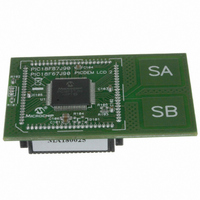
MA180025 Microchip Technology, MA180025 Datasheet - Page 287

MA180025
Manufacturer Part Number
MA180025
Description
MODULE PLUG-IN PIC18F87J90 PIM
Manufacturer
Microchip Technology
Series
PIC®r
Specifications of MA180025
Accessory Type
Plug-In Module (PIM) - PIC18F87J90
Product
Microcontroller Modules
Silicon Manufacturer
Microchip
Core Architecture
PIC
Core Sub-architecture
PIC18
Silicon Core Number
PIC18F
Silicon Family Name
PIC18FxxJxx
Lead Free Status / RoHS Status
Lead free / RoHS Compliant
For Use With/related Products
PICDEM LCD 2 Demonstration Board (DM163030)
For Use With
DM163030 - KIT DEV PICDEM LCD2
Lead Free Status / Rohs Status
Lead free / RoHS Compliant
Available stocks
Company
Part Number
Manufacturer
Quantity
Price
Company:
Part Number:
MA180025
Manufacturer:
Microchip Technology
Quantity:
135
Company:
Part Number:
MA180025
Manufacturer:
MICROCHIP
Quantity:
12 000
- Current page: 287 of 450
- Download datasheet (4Mb)
20.5
Synchronous Slave mode is entered by clearing bit,
CSRC (TXSTA2<7>). This mode differs from the
Synchronous Master mode in that the shift clock is
supplied externally at the CK2 pin (instead of being
supplied internally in Master mode). This allows the
device to transfer or receive data while in any
Low-Power mode.
20.5.1
The operation of the Synchronous Master and Slave
modes are identical except in the case of the Sleep
mode.
If two words are written to the TXREG2 and then the
SLEEP instruction is executed, the following will occur:
a)
b)
c)
d)
e)
TABLE 20-8:
2010 Microchip Technology Inc.
INTCON
PIR3
PIE3
IPR3
RCSTA2
TXREG2
TXSTA2
SPBRG2
LATG
Legend: — = unimplemented, read as ‘0’. Shaded cells are not used for synchronous slave transmission.
Name
The first word will immediately transfer to the
TSR register and transmit.
The second word will remain in the TXREG2
register.
Flag bit, TX2IF, will not be set.
When the first word has been shifted out of TSR,
the TXREG2 register will transfer the second
word to the TSR and flag bit, TX2IF, will now be
set.
If enable bit, TX2IE, is set, the interrupt will wake
the chip from Sleep. If the global interrupt is
enabled, the program will branch to the interrupt
vector.
AUSART Synchronous Slave Mode
AUSART SYNCHRONOUS
SLAVE TRANSMIT
AUSART Transmit Register
AUSART Baud Rate Generator Register
GIE/GIEH PEIE/GIEL
CSRC
U2OD
SPEN
Bit 7
REGISTERS ASSOCIATED WITH SYNCHRONOUS SLAVE TRANSMISSION
—
—
—
LCDIF
LCDIE
LCDIP
U1OD
Bit 6
RX9
TX9
TMR0IE
RC2IF
RC2IE
RC2IP
SREN
TXEN
Bit 5
—
INT0IE
LATG4
TX2IE
TX2IP
CREN
SYNC
TX2IF
Bit 4
PIC18F87J90 FAMILY
CTMUIF
CTMUIE
CTMUIP
ADDEN
To set up a Synchronous Slave Transmission:
1.
2.
3.
4.
5.
6.
7.
8.
LATG3
RBIE
Bit 3
—
Enable the synchronous slave serial port by
setting bits, SYNC and SPEN, and clearing bit,
CSRC.
Clear bits, CREN and SREN.
If interrupts are desired, set enable bit, TX2IE.
If 9-bit transmission is desired, set bit, TX9.
Enable the transmission by setting enable bit,
TXEN.
If 9-bit transmission is selected, the ninth bit
should be loaded in bit, TX9D.
Start transmission by loading data to the
TXREG2 register.
If using interrupts, ensure that the GIE and PEIE
bits in the INTCON register (INTCON<7:6>) are
set.
TMR0IF
CCP2IF
CCP2IE
CCP2IP
LATG2
BRGH
FERR
Bit 2
CCP1IF
CCP1IE
CCP1IP
INT0IF
LATG1
OERR
TRMT
Bit 1
RTCCIF
RTCCIE
RTCCIP
LATG0
RX9D
TX9D
DS39933D-page 287
RBIF
Bit 0
on Page
Values
Reset
59
62
62
62
64
64
64
64
62
Related parts for MA180025
Image
Part Number
Description
Manufacturer
Datasheet
Request
R

Part Number:
Description:
Manufacturer:
Microchip Technology Inc.
Datasheet:

Part Number:
Description:
Manufacturer:
Microchip Technology Inc.
Datasheet:

Part Number:
Description:
Manufacturer:
Microchip Technology Inc.
Datasheet:

Part Number:
Description:
Manufacturer:
Microchip Technology Inc.
Datasheet:

Part Number:
Description:
Manufacturer:
Microchip Technology Inc.
Datasheet:

Part Number:
Description:
Manufacturer:
Microchip Technology Inc.
Datasheet:

Part Number:
Description:
Manufacturer:
Microchip Technology Inc.
Datasheet:

Part Number:
Description:
Manufacturer:
Microchip Technology Inc.
Datasheet:


