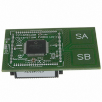
MA180025 Microchip Technology, MA180025 Datasheet - Page 87

MA180025
Manufacturer Part Number
MA180025
Description
MODULE PLUG-IN PIC18F87J90 PIM
Manufacturer
Microchip Technology
Series
PIC®r
Specifications of MA180025
Accessory Type
Plug-In Module (PIM) - PIC18F87J90
Product
Microcontroller Modules
Silicon Manufacturer
Microchip
Core Architecture
PIC
Core Sub-architecture
PIC18
Silicon Core Number
PIC18F
Silicon Family Name
PIC18FxxJxx
Lead Free Status / RoHS Status
Lead free / RoHS Compliant
For Use With/related Products
PICDEM LCD 2 Demonstration Board (DM163030)
For Use With
DM163030 - KIT DEV PICDEM LCD2
Lead Free Status / Rohs Status
Lead free / RoHS Compliant
Available stocks
Company
Part Number
Manufacturer
Quantity
Price
Company:
Part Number:
MA180025
Manufacturer:
Microchip Technology
Quantity:
135
Company:
Part Number:
MA180025
Manufacturer:
MICROCHIP
Quantity:
12 000
- Current page: 87 of 450
- Download datasheet (4Mb)
6.6.3
The use of Indexed Literal Offset Addressing mode
effectively changes how the lower part of Access RAM
(00h to 5Fh) is mapped. Rather than containing just the
contents of the bottom part of Bank 0, this mode maps
the contents from Bank 0 and a user-defined “window”
that can be located anywhere in the data memory
space. The value of FSR2 establishes the lower bound-
ary of the addresses mapped into the window, while the
upper boundary is defined by FSR2 plus 95 (5Fh).
Addresses in the Access RAM above 5Fh are mapped
as previously described (see Section 6.3.2 “Access
Bank”). An example of Access Bank remapping in this
addressing mode is shown in Figure 6-10.
FIGURE 6-10:
2010 Microchip Technology Inc.
Example Situation:
ADDWF f, d, a
FSR2H:FSR2L = 120h
Locations in the region
from the FSR2 Pointer
(120h) to the pointer plus
05Fh (17Fh) are mapped
to
Access RAM (000h-05Fh).
Special Function Registers
at F60h through FFFh are
mapped to 60h through
FFh, as usual.
Bank 0 addresses below
5Fh are not available in
this mode. They can still
be addressed by using the
BSR.
the
MAPPING THE ACCESS BANK IN
INDEXED LITERAL OFFSET MODE
bottom
of
REMAPPING THE ACCESS BANK WITH INDEXED LITERAL
OFFSET ADDRESSING
the
FFFh
05Fh
17Fh
F00h
F60h
000h
100h
120h
200h
Data Memory
Not Accessible
Bank 14
Bank 15
Window
through
Bank 0
Bank 1
Bank 2
SFRs
PIC18F87J90 FAMILY
Remapping of the Access Bank applies only to opera-
tions using the Indexed Literal Offset mode. Operations
that use the BSR (Access RAM bit is ‘1’) will continue
to use Direct Addressing as before. Any Indirect or
Indexed Addressing operation that explicitly uses any
of the indirect file operands (including FSR2) will con-
tinue to operate as standard Indirect Addressing. Any
instruction that uses the Access Bank, but includes a
register address of greater than 05Fh, will use Direct
Addressing and the normal Access Bank map.
6.6.4
Although the Access Bank is remapped when the
extended instruction set is enabled, the operation of the
BSR remains unchanged. Direct Addressing, using the
BSR to select the data memory bank, operates in the
same manner as previously described.
BSR IN INDEXED LITERAL
OFFSET MODE
Bank 1 “Window”
Access Bank
SFRs
DS39933D-page 87
00h
5Fh
60h
FFh
Related parts for MA180025
Image
Part Number
Description
Manufacturer
Datasheet
Request
R

Part Number:
Description:
Manufacturer:
Microchip Technology Inc.
Datasheet:

Part Number:
Description:
Manufacturer:
Microchip Technology Inc.
Datasheet:

Part Number:
Description:
Manufacturer:
Microchip Technology Inc.
Datasheet:

Part Number:
Description:
Manufacturer:
Microchip Technology Inc.
Datasheet:

Part Number:
Description:
Manufacturer:
Microchip Technology Inc.
Datasheet:

Part Number:
Description:
Manufacturer:
Microchip Technology Inc.
Datasheet:

Part Number:
Description:
Manufacturer:
Microchip Technology Inc.
Datasheet:

Part Number:
Description:
Manufacturer:
Microchip Technology Inc.
Datasheet:


