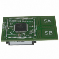
MA180025 Microchip Technology, MA180025 Datasheet - Page 21

MA180025
Manufacturer Part Number
MA180025
Description
MODULE PLUG-IN PIC18F87J90 PIM
Manufacturer
Microchip Technology
Series
PIC®r
Specifications of MA180025
Accessory Type
Plug-In Module (PIM) - PIC18F87J90
Product
Microcontroller Modules
Silicon Manufacturer
Microchip
Core Architecture
PIC
Core Sub-architecture
PIC18
Silicon Core Number
PIC18F
Silicon Family Name
PIC18FxxJxx
Lead Free Status / RoHS Status
Lead free / RoHS Compliant
For Use With/related Products
PICDEM LCD 2 Demonstration Board (DM163030)
For Use With
DM163030 - KIT DEV PICDEM LCD2
Lead Free Status / Rohs Status
Lead free / RoHS Compliant
Available stocks
Company
Part Number
Manufacturer
Quantity
Price
Company:
Part Number:
MA180025
Manufacturer:
Microchip Technology
Quantity:
135
Company:
Part Number:
MA180025
Manufacturer:
MICROCHIP
Quantity:
12 000
- Current page: 21 of 450
- Download datasheet (4Mb)
TABLE 1-4:
2010 Microchip Technology Inc.
MCLR
OSC1/CLKI/RA7
OSC2/CLKO/RA6
RA0/AN0
RA1/AN1/SEG18
RA2/AN2/V
RA3/AN3/V
RA4/T0CKI/SEG14
RA5/AN4/SEG15
RA6
RA7
Legend: TTL = TTL compatible input
Note 1:
OSC1
CLKI
RA7
OSC2
CLKO
RA6
RA0
AN0
RA1
AN1
SEG18
RA2
AN2
V
RA3
AN3
V
RA4
T0CKI
SEG14
RA5
AN4
SEG15
REF
REF
2:
Pin Name
-
+
ST
I
P
I
Default assignment for CCP2 when the CCP2MX Configuration bit is set.
Alternate assignment for CCP2 when the CCP2MX Configuration bit is cleared.
REF
REF
2
C™ = I
-
+
= Schmitt Trigger input with CMOS levels
= Input
= Power
PIC18F8XJ90 PINOUT I/O DESCRIPTIONS
2
C/SMBus
Pin Number
TQFP
49
50
30
29
28
27
34
33
9
Type
Pin
I/O
I/O
I/O
I/O
I/O
I/O
I/O
I/O
O
O
O
O
O
I
I
I
I
I
I
I
I
I
I
I
CMOS
CMOS
Analog
Analog
Analog
Analog
Analog
Analog
Analog
Analog
Analog
Analog
Buffer
Type
TTL
TTL
TTL
TTL
TTL
TTL
TTL
ST
ST
ST
—
—
Master Clear (input) or programming voltage (input). This
pin is an active-low Reset to the device.
Oscillator crystal or external clock input.
Oscillator crystal or clock output.
PORTA is a bidirectional I/O port.
Oscillator crystal input.
External clock source input. Always associated
with pin function, OSC1. (See related OSC1/CLKI,
OSC2/CLKO pins.)
General purpose I/O pin.
Oscillator crystal output. Connects to crystal or
resonator in Crystal Oscillator mode.
In EC modes, OSC2 pin outputs CLKO, which has
1/4 the frequency of OSC1 and denotes the
instruction cycle rate.
General purpose I/O pin.
Digital I/O.
Analog Input 0.
Digital I/O.
Analog Input 1.
SEG18 output for LCD.
Digital I/O.
Analog Input 2.
A/D reference voltage (low) input.
Digital I/O.
Analog Input 3.
A/D reference voltage (high) input.
Digital I/O.
Timer0 external clock input.
SEG14 output for LCD.
Digital I/O.
Analog Input 4.
SEG15 output for LCD.
See the OSC2/CLKO/RA6 pin.
See the OSC1/CLKI/RA7 pin.
PIC18F87J90 FAMILY
CMOS = CMOS compatible input or output
Analog = Analog input
O
OD
= Output
= Open-Drain (no P diode to V
Description
DS39933D-page 21
DD
)
Related parts for MA180025
Image
Part Number
Description
Manufacturer
Datasheet
Request
R

Part Number:
Description:
Manufacturer:
Microchip Technology Inc.
Datasheet:

Part Number:
Description:
Manufacturer:
Microchip Technology Inc.
Datasheet:

Part Number:
Description:
Manufacturer:
Microchip Technology Inc.
Datasheet:

Part Number:
Description:
Manufacturer:
Microchip Technology Inc.
Datasheet:

Part Number:
Description:
Manufacturer:
Microchip Technology Inc.
Datasheet:

Part Number:
Description:
Manufacturer:
Microchip Technology Inc.
Datasheet:

Part Number:
Description:
Manufacturer:
Microchip Technology Inc.
Datasheet:

Part Number:
Description:
Manufacturer:
Microchip Technology Inc.
Datasheet:


