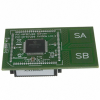
MA180025 Microchip Technology, MA180025 Datasheet - Page 187

MA180025
Manufacturer Part Number
MA180025
Description
MODULE PLUG-IN PIC18F87J90 PIM
Manufacturer
Microchip Technology
Series
PIC®r
Specifications of MA180025
Accessory Type
Plug-In Module (PIM) - PIC18F87J90
Product
Microcontroller Modules
Silicon Manufacturer
Microchip
Core Architecture
PIC
Core Sub-architecture
PIC18
Silicon Core Number
PIC18F
Silicon Family Name
PIC18FxxJxx
Lead Free Status / RoHS Status
Lead free / RoHS Compliant
For Use With/related Products
PICDEM LCD 2 Demonstration Board (DM163030)
For Use With
DM163030 - KIT DEV PICDEM LCD2
Lead Free Status / Rohs Status
Lead free / RoHS Compliant
Available stocks
Company
Part Number
Manufacturer
Quantity
Price
Company:
Part Number:
MA180025
Manufacturer:
Microchip Technology
Quantity:
135
Company:
Part Number:
MA180025
Manufacturer:
MICROCHIP
Quantity:
12 000
- Current page: 187 of 450
- Download datasheet (4Mb)
17.1.2
Once the module is initialized for the LCD panel, the
individual bits of the LCDDATA23:LCDDATA0 registers
are cleared or set to represent a clear or dark pixel,
respectively. Specific sets of LCDDATA registers are
used with specific segments and common signals.
Each bit represents a unique combination of a specific
segment connected to a specific common.
REGISTER 17-4:
TABLE 17-2:
2010 Microchip Technology Inc.
bit 7
Legend:
R = Readable bit
-n = Value at POR
bit 7-0
Note 1:
S(n + 7)Cy
16 through 23
24 through 31
32 through 39
40 through 47
8 through 15
R/W-0
0 through 7
Segments
2:
Bits<7:1> of these registers are not implemented in PIC18F6XJ90 devices. Bit 0 of these registers
(SEG32Cy) is always implemented.
These registers are not implemented on PIC18F6XJ90 devices.
LCD DATA REGISTERS
S(n + 7)Cy:S(n)Cy: Pixel On bits
For LCDDATA0 through LCDDATA5: n = (8x), y = 0
For LCDDATA6 through LCDDATA11: n = (8(x – 6)), y = 1
For LCDDATA12 through LCDDATA17: n = (8(x – 12)), y = 2
For LCDDATA18 through LCDDATA23: n = (8(x – 18)), y = 3
1 = Pixel on (dark)
0 = Pixel off (clear)
S(n + 6)Cy
LCDDATA REGISTERS AND BITS FOR SEGMENT AND COM COMBINATIONS
R/W-0
LCDDATAx: LCD DATA REGISTERS
S00C0:S07C0
S08C0:S15C0
S16C0:S23C0
S24C0:S31C0
S32C0:S39C0
S40C0:S47C0
LCDDATA4
LCDDATA5
LCDDATA0
LCDDATA1
LCDDATA2
LCDDATA3
W = Writable bit
‘1’ = Bit is set
S(n + 5)Cy
0
R/W-0
(1)
(2)
S(n + 4)Cy
R/W-0
LCDDATA10
LCDDATA11
S00C1:S07C1
S08C1:S15C1
S16C1:S23C1
S24C1:S31C1
S32C1:S39C1
S40C1:S47C1
LCDDATA6
LCDDATA7
LCDDATA8
LCDDATA9
1
U = Unimplemented bit, read as ‘0’
‘0’ = Bit is cleared
S(n + 3)Cy
PIC18F87J90 FAMILY
(2)
(1)
COM Lines
R/W-0
Individual LCDDATA bits are named by the convention
“SxxCy”, with “xx” as the segment number and “y” as
the common number. The relationship is summarized
in Table 17-2. The prototype LCDDATA register is
shown in Register 17-4.
Note:
LCDDATA16
LCDDATA17
S00C2:S07C2
S08C2:S15C2
S16C2:S23C2
S24C2:S31C2
S32C2:S39C2
S40C2:S47C2
LCDDATA12
LCDDATA13
LCDDATA14
LCDDATA15
In 64-pin devices, writing into the registers
LCDDATA5, LCDDATA11, LCDDATA17
and LCDDATA23, will not affect the status
of any pixels.
S(n + 2)Cy
R/W-0
2
(1)
(2)
x = Bit is unknown
S(n + 1)Cy
R/W-0
LCDDATA22
LCDDATA23
S00C3:S07C3
S08C0:S15C3
S16C3:S23C3
S24C3:S31C3
S32C3:S39C3
S40C3:S47C3
DS39933D-page 187
LCDDATA18
LCDDATA19
LCDDATA20
LCDDATA21
3
S(n)Cy
R/W-0
(1)
(2)
bit 0
Related parts for MA180025
Image
Part Number
Description
Manufacturer
Datasheet
Request
R

Part Number:
Description:
Manufacturer:
Microchip Technology Inc.
Datasheet:

Part Number:
Description:
Manufacturer:
Microchip Technology Inc.
Datasheet:

Part Number:
Description:
Manufacturer:
Microchip Technology Inc.
Datasheet:

Part Number:
Description:
Manufacturer:
Microchip Technology Inc.
Datasheet:

Part Number:
Description:
Manufacturer:
Microchip Technology Inc.
Datasheet:

Part Number:
Description:
Manufacturer:
Microchip Technology Inc.
Datasheet:

Part Number:
Description:
Manufacturer:
Microchip Technology Inc.
Datasheet:

Part Number:
Description:
Manufacturer:
Microchip Technology Inc.
Datasheet:


