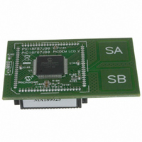
MA180025 Microchip Technology, MA180025 Datasheet - Page 184

MA180025
Manufacturer Part Number
MA180025
Description
MODULE PLUG-IN PIC18F87J90 PIM
Manufacturer
Microchip Technology
Series
PIC®r
Specifications of MA180025
Accessory Type
Plug-In Module (PIM) - PIC18F87J90
Product
Microcontroller Modules
Silicon Manufacturer
Microchip
Core Architecture
PIC
Core Sub-architecture
PIC18
Silicon Core Number
PIC18F
Silicon Family Name
PIC18FxxJxx
Lead Free Status / RoHS Status
Lead free / RoHS Compliant
For Use With/related Products
PICDEM LCD 2 Demonstration Board (DM163030)
For Use With
DM163030 - KIT DEV PICDEM LCD2
Lead Free Status / Rohs Status
Lead free / RoHS Compliant
Available stocks
Company
Part Number
Manufacturer
Quantity
Price
Company:
Part Number:
MA180025
Manufacturer:
Microchip Technology
Quantity:
135
Company:
Part Number:
MA180025
Manufacturer:
MICROCHIP
Quantity:
12 000
- Current page: 184 of 450
- Download datasheet (4Mb)
PIC18F87J90 FAMILY
17.1
The LCD driver module has 33 registers:
• LCD Control Register (LCDCON)
• LCD Phase Register (LCDPS)
• LCDREG Register (LCD Regulator Control)
• Six LCD Segment Enable Registers
• 24 LCD Data Registers
17.1.1
The LCDCON register, shown in Register 17-1,
controls the overall operation of the module. Once the
module is configured, the LCDEN (LCDCON<7>) bit is
used to enable or disable the LCD module. The LCD
panel can also operate during Sleep by clearing the
SLPEN (LCDCON<6>) bit.
REGISTER 17-1:
DS39933D-page 184
bit 7
Legend:
R = Readable bit
-n = Value at POR
bit 7
bit 6
bit 5
bit 4
bit 3-2
bit 1-0
(LCDSE5:LCDSE0)
(LCDDATA23:LCDDATA0)
LCDEN
R/W-0
LCD Registers
LCD CONTROL REGISTERS
LCDEN: LCD Driver Enable bit
1 = LCD driver module is enabled
0 = LCD driver module is disabled
SLPEN: LCD Driver Enable in Sleep mode bit
1 = LCD driver module is disabled in Sleep mode
0 = LCD driver module is enabled in Sleep mode
WERR: LCD Write Failed Error bit
1 = LCDDATAx register written while LCDPS<4> = 0 (must be cleared in software)
0 = No LCD write error
Unimplemented: Read as ‘0’
CS<1:0>: Clock Source Select bits
1x = INTRC (31 kHz)
01 = T13CKI (Timer1)
00 = System clock (F
LMUX<1:0>: Commons Select bits
LMUX<1:0>
SLPEN
R/W-0
00
01
10
11
LCDCON: LCD CONTROL REGISTER
C = Clearable bit
W = Writable bit
‘1’ = Bit is set
1/2 (COM1:COM0)
1/3 (COM2:COM0)
1/4 (COM3:COM0)
WERR
R/C-0
Multiplex Type
Static (COM0)
OSC
/4)
U-0
—
PIC18F6XJ90
Maximum Number of Pixels:
U = Unimplemented bit, read as ‘0’
‘0’ = Bit is cleared
132
R/W-0
33
66
99
The
configures the LCD clock source prescaler and the type
of waveform: Type-A or Type-B. Details on these
features are provided in Section 17.2 “LCD Clock
Source”, Section 17.3 “LCD Bias Generation” and
Section 17.8 “LCD Waveform Generation”.
The LCDREG register is described in Section 17.3
“LCD Bias Generation”.
The LCD Segment Enable registers (LCDSEx)
configure the functions of the port pins. Setting the
segment enable bit for a particular segment configures
that pin as an LCD driver. The prototype LCDSE register
is shown in Register 17-3. There are six LCDSE
registers (LCDSE5:LCDSE0) listed in Table 17-1.
CS1
LCDPS
PIC18F8XJ90
R/W-0
CS0
register,
144
192
48
96
2010 Microchip Technology Inc.
x = Bit is unknown
shown
LMUX1
R/W-0
Bias Type
in
1/2 or 1/3
1/2 or 1/3
Static
1/3
Register 17-2,
LMUX0
R/W-0
bit 0
Related parts for MA180025
Image
Part Number
Description
Manufacturer
Datasheet
Request
R

Part Number:
Description:
Manufacturer:
Microchip Technology Inc.
Datasheet:

Part Number:
Description:
Manufacturer:
Microchip Technology Inc.
Datasheet:

Part Number:
Description:
Manufacturer:
Microchip Technology Inc.
Datasheet:

Part Number:
Description:
Manufacturer:
Microchip Technology Inc.
Datasheet:

Part Number:
Description:
Manufacturer:
Microchip Technology Inc.
Datasheet:

Part Number:
Description:
Manufacturer:
Microchip Technology Inc.
Datasheet:

Part Number:
Description:
Manufacturer:
Microchip Technology Inc.
Datasheet:

Part Number:
Description:
Manufacturer:
Microchip Technology Inc.
Datasheet:


