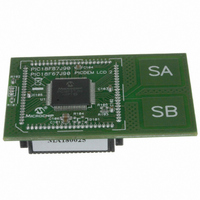
MA180025 Microchip Technology, MA180025 Datasheet - Page 215

MA180025
Manufacturer Part Number
MA180025
Description
MODULE PLUG-IN PIC18F87J90 PIM
Manufacturer
Microchip Technology
Series
PIC®r
Specifications of MA180025
Accessory Type
Plug-In Module (PIM) - PIC18F87J90
Product
Microcontroller Modules
Silicon Manufacturer
Microchip
Core Architecture
PIC
Core Sub-architecture
PIC18
Silicon Core Number
PIC18F
Silicon Family Name
PIC18FxxJxx
Lead Free Status / RoHS Status
Lead free / RoHS Compliant
For Use With/related Products
PICDEM LCD 2 Demonstration Board (DM163030)
For Use With
DM163030 - KIT DEV PICDEM LCD2
Lead Free Status / Rohs Status
Lead free / RoHS Compliant
Available stocks
Company
Part Number
Manufacturer
Quantity
Price
Company:
Part Number:
MA180025
Manufacturer:
Microchip Technology
Quantity:
135
Company:
Part Number:
MA180025
Manufacturer:
MICROCHIP
Quantity:
12 000
- Current page: 215 of 450
- Download datasheet (4Mb)
18.3.3
To enable the serial port, the MSSP Enable bit, SSPEN
(SSPCON1<5>), must be set. To reset or reconfigure
SPI mode, clear the SSPEN bit, reinitialize the
SSPCON registers and then set the SSPEN bit. This
configures the SDI, SDO, SCK and SS pins as serial
port pins. For the pins to behave as the serial port func-
tion, some must have their data direction bits (in the
TRIS register) appropriately programmed as follows:
• SDI is automatically controlled by the SPI module
• SDO must have TRISC<5> bit cleared
• SCK (Master mode) must have TRISC<3> bit
• SCK (Slave mode) must have TRISC<3> bit set
• SS must have TRISF<7> bit set
Any serial port function that is not desired may be
overridden by programming the corresponding data
direction (TRIS) register to the opposite value.
18.3.4
The drivers for the SDO output and SCK clock pins can
be optionally configured as open-drain outputs. This
feature allows the voltage level on the pin to be pulled
FIGURE 18-2:
2010 Microchip Technology Inc.
cleared
ENABLING SPI I/O
OPEN-DRAIN OUTPUT OPTION
SPI Master SSPM<3:0> =
MSb
PROCESSOR 1
Serial Input Buffer
SPI MASTER/SLAVE CONNECTION
Shift Register
(SSPBUF)
(SSPSR)
00xx
LSb
SDO
SCK
SDI
Serial Clock
PIC18F87J90 FAMILY
to a higher level through an external pull-up resistor,
and allows the output to communicate with external
circuits without the need for additional level shifters.
The open-drain output option is controlled by the
SPIOD bit (TRISG<7>). Setting this bit configures both
pins for open-drain operation.
18.3.5
Figure 18-2 shows a typical connection between two
microcontrollers. The master controller (Processor 1)
initiates the data transfer by sending the SCK signal.
Data is shifted out of both shift registers on their pro-
grammed clock edge and latched on the opposite edge
of the clock. Both processors should be programmed to
the same Clock Polarity (CKP), then both controllers
would send and receive data at the same time.
Whether the data is meaningful (or dummy data)
depends on the application software. This leads to
three scenarios for data transmission:
• Master sends data–Slave sends dummy data
• Master sends data–Slave sends data
• Master sends dummy data–Slave sends data
SDO
SCK
SDI
TYPICAL CONNECTION
SPI Slave SSPM<3:0> =
MSb
Serial Input Buffer
Shift Register
PROCESSOR 2
(SSPBUF)
(SSPSR)
LSb
DS39933D-page 215
010x
Related parts for MA180025
Image
Part Number
Description
Manufacturer
Datasheet
Request
R

Part Number:
Description:
Manufacturer:
Microchip Technology Inc.
Datasheet:

Part Number:
Description:
Manufacturer:
Microchip Technology Inc.
Datasheet:

Part Number:
Description:
Manufacturer:
Microchip Technology Inc.
Datasheet:

Part Number:
Description:
Manufacturer:
Microchip Technology Inc.
Datasheet:

Part Number:
Description:
Manufacturer:
Microchip Technology Inc.
Datasheet:

Part Number:
Description:
Manufacturer:
Microchip Technology Inc.
Datasheet:

Part Number:
Description:
Manufacturer:
Microchip Technology Inc.
Datasheet:

Part Number:
Description:
Manufacturer:
Microchip Technology Inc.
Datasheet:


