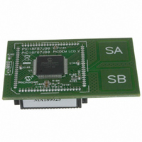
MA180025 Microchip Technology, MA180025 Datasheet - Page 292

MA180025
Manufacturer Part Number
MA180025
Description
MODULE PLUG-IN PIC18F87J90 PIM
Manufacturer
Microchip Technology
Series
PIC®r
Specifications of MA180025
Accessory Type
Plug-In Module (PIM) - PIC18F87J90
Product
Microcontroller Modules
Silicon Manufacturer
Microchip
Core Architecture
PIC
Core Sub-architecture
PIC18
Silicon Core Number
PIC18F
Silicon Family Name
PIC18FxxJxx
Lead Free Status / RoHS Status
Lead free / RoHS Compliant
For Use With/related Products
PICDEM LCD 2 Demonstration Board (DM163030)
For Use With
DM163030 - KIT DEV PICDEM LCD2
Lead Free Status / Rohs Status
Lead free / RoHS Compliant
Available stocks
Company
Part Number
Manufacturer
Quantity
Price
Company:
Part Number:
MA180025
Manufacturer:
Microchip Technology
Quantity:
135
Company:
Part Number:
MA180025
Manufacturer:
MICROCHIP
Quantity:
12 000
- Current page: 292 of 450
- Download datasheet (4Mb)
PIC18F87J90 FAMILY
The analog reference voltage is software selectable to
either the device’s positive and negative supply voltage
(AV
RA3/AN3/V
The A/D Converter has a unique feature of being able
to operate while the device is in Sleep mode. To
operate in Sleep, the A/D conversion clock must be
derived from the A/D’s Internal RC oscillator.
The output of the sample and hold is the input into the
converter, which generates the result via successive
approximation.
Each port pin associated with the A/D Converter can be
configured as an analog input or as a digital I/O. The
ADRESH and ADRESL registers contain the result of
FIGURE 21-1:
DS39933D-page 292
DD
Note 1: Channels, AN15 through AN12, are not available on PIC18F6XJ90 devices.
and AV
REF
2: I/O pins have diode protection to V
Converter
+ and RA2/AN2/V
10-Bit
SS
A/D
), or the voltage level on the
Reference
Voltage
A/D BLOCK DIAGRAM
REF
- pins.
V
V
REF
REF
+
-
(Input Voltage)
VCFG<1:0>
V
(1,2)
AIN
DD
and V
AV
SS
DD
.
the A/D conversion. When the A/D conversion is com-
plete, the result is loaded into the ADRESH:ADRESL
register pair, the GO/DONE bit (ADCON0<1>) is
cleared and the A/D Interrupt Flag bit, ADIF, is set.
A device Reset forces all registers to their Reset state.
This forces the A/D module to be turned off and any
conversion in progress is aborted. The value in the
ADRESH:ADRESL register pair is not modified for a
Power-on Reset. These registers will contain unknown
data after a Power-on Reset.
The block diagram of the A/D module is shown in
Figure 21-1.
AV
SS
CHS<3:0>
1011
1010
1001
1000
0111
0110
0101
0100
0011
0010
0001
0000
2010 Microchip Technology Inc.
AN11
AN10
AN9
AN8
AN7
AN6
AN5
AN4
AN3
AN2
AN1
AN0
Related parts for MA180025
Image
Part Number
Description
Manufacturer
Datasheet
Request
R

Part Number:
Description:
Manufacturer:
Microchip Technology Inc.
Datasheet:

Part Number:
Description:
Manufacturer:
Microchip Technology Inc.
Datasheet:

Part Number:
Description:
Manufacturer:
Microchip Technology Inc.
Datasheet:

Part Number:
Description:
Manufacturer:
Microchip Technology Inc.
Datasheet:

Part Number:
Description:
Manufacturer:
Microchip Technology Inc.
Datasheet:

Part Number:
Description:
Manufacturer:
Microchip Technology Inc.
Datasheet:

Part Number:
Description:
Manufacturer:
Microchip Technology Inc.
Datasheet:

Part Number:
Description:
Manufacturer:
Microchip Technology Inc.
Datasheet:


