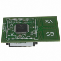
MA180025 Microchip Technology, MA180025 Datasheet - Page 282

MA180025
Manufacturer Part Number
MA180025
Description
MODULE PLUG-IN PIC18F87J90 PIM
Manufacturer
Microchip Technology
Series
PIC®r
Specifications of MA180025
Accessory Type
Plug-In Module (PIM) - PIC18F87J90
Product
Microcontroller Modules
Silicon Manufacturer
Microchip
Core Architecture
PIC
Core Sub-architecture
PIC18
Silicon Core Number
PIC18F
Silicon Family Name
PIC18FxxJxx
Lead Free Status / RoHS Status
Lead free / RoHS Compliant
For Use With/related Products
PICDEM LCD 2 Demonstration Board (DM163030)
For Use With
DM163030 - KIT DEV PICDEM LCD2
Lead Free Status / Rohs Status
Lead free / RoHS Compliant
Available stocks
Company
Part Number
Manufacturer
Quantity
Price
Company:
Part Number:
MA180025
Manufacturer:
Microchip Technology
Quantity:
135
Company:
Part Number:
MA180025
Manufacturer:
MICROCHIP
Quantity:
12 000
- Current page: 282 of 450
- Download datasheet (4Mb)
PIC18F87J90 FAMILY
20.3.2
The receiver block diagram is shown in Figure 20-4.
The data is received on the RX2 pin and drives the data
recovery block. The data recovery block is actually a
high-speed shifter operating at x16 times the baud rate,
whereas the main receive serial shifter operates at the
bit rate or at F
in RS-232 systems.
To set up an Asynchronous Reception:
1.
2.
3.
4.
5.
6.
7.
8.
9.
10. If using interrupts, ensure that the GIE and PEIE
FIGURE 20-4:
DS39933D-page 282
Initialize the SPBRG2 register for the appropriate
baud rate. Set or clear the BRGH bit, as required,
to achieve the desired baud rate.
Enable the asynchronous serial port by clearing
bit, SYNC, and setting bit, SPEN.
If interrupts are desired, set enable bit, RC2IE.
If 9-bit reception is desired, set bit, RX9.
Enable the reception by setting bit, CREN.
Flag bit, RC2IF, will be set when reception is
complete and an interrupt will be generated if
enable bit, RC2IE, was set.
Read the RCSTA2 register to get the 9th bit (if
enabled) and determine if any error occurred
during reception.
Read the 8-bit received data by reading the
RCREG2 register.
If any error occurred, clear the error by clearing
enable bit, CREN.
bits in the INTCON register (INTCON<7:6>) are
set.
AUSART ASYNCHRONOUS
RECEIVER
RX2
OSC
. This mode would typically be used
AUSART RECEIVE BLOCK DIAGRAM
and Control
Pin Buffer
Baud Rate Generator
x64 Baud Rate CLK
SPEN
SPBRG2
Recovery
Interrupt
64
16
Data
4
or
or
CREN
20.3.3
This mode would typically be used in RS-485 systems.
To set up an Asynchronous Reception with Address
Detect Enable:
1.
2.
3.
4.
5.
6.
7.
8.
9.
10. If any error occurred, clear the CREN bit.
11. If the device has been addressed, clear the
RX9
Initialize the SPBRG2 register for the appropriate
baud rate. Set or clear the BRGH and BRG16
bits, as required, to achieve the desired baud
rate.
Enable the asynchronous serial port by clearing
the SYNC bit and setting the SPEN bit.
If interrupts are required, set the RCEN bit and
select the desired priority level with the RC2IP
bit.
Set the RX9 bit to enable 9-bit reception.
Set the ADDEN bit to enable address detect.
Enable reception by setting the CREN bit.
The RC2IF bit will be set when reception is
complete. The interrupt will be Acknowledged if
the RC2IE and GIE bits are set.
Read the RCSTA2 register to determine if any
error occurred during reception, as well as read
bit 9 of data (if applicable).
Read RCREG2 to determine if the device is
being addressed.
ADDEN bit to allow all received data into the
receive buffer and interrupt the CPU.
Stop
MSb
RC2IF
RC2IE
RX9D
SETTING UP 9-BIT MODE WITH
ADDRESS DETECT
(8)
OERR
7
RSR Register
RCREG2 Register
2010 Microchip Technology Inc.
8
Data Bus
1
FERR
0
LSb
Start
FIFO
Related parts for MA180025
Image
Part Number
Description
Manufacturer
Datasheet
Request
R

Part Number:
Description:
Manufacturer:
Microchip Technology Inc.
Datasheet:

Part Number:
Description:
Manufacturer:
Microchip Technology Inc.
Datasheet:

Part Number:
Description:
Manufacturer:
Microchip Technology Inc.
Datasheet:

Part Number:
Description:
Manufacturer:
Microchip Technology Inc.
Datasheet:

Part Number:
Description:
Manufacturer:
Microchip Technology Inc.
Datasheet:

Part Number:
Description:
Manufacturer:
Microchip Technology Inc.
Datasheet:

Part Number:
Description:
Manufacturer:
Microchip Technology Inc.
Datasheet:

Part Number:
Description:
Manufacturer:
Microchip Technology Inc.
Datasheet:


