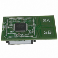
MA180025 Microchip Technology, MA180025 Datasheet - Page 190

MA180025
Manufacturer Part Number
MA180025
Description
MODULE PLUG-IN PIC18F87J90 PIM
Manufacturer
Microchip Technology
Series
PIC®r
Specifications of MA180025
Accessory Type
Plug-In Module (PIM) - PIC18F87J90
Product
Microcontroller Modules
Silicon Manufacturer
Microchip
Core Architecture
PIC
Core Sub-architecture
PIC18
Silicon Core Number
PIC18F
Silicon Family Name
PIC18FxxJxx
Lead Free Status / RoHS Status
Lead free / RoHS Compliant
For Use With/related Products
PICDEM LCD 2 Demonstration Board (DM163030)
For Use With
DM163030 - KIT DEV PICDEM LCD2
Lead Free Status / Rohs Status
Lead free / RoHS Compliant
Available stocks
Company
Part Number
Manufacturer
Quantity
Price
Company:
Part Number:
MA180025
Manufacturer:
Microchip Technology
Quantity:
135
Company:
Part Number:
MA180025
Manufacturer:
MICROCHIP
Quantity:
12 000
- Current page: 190 of 450
- Download datasheet (4Mb)
PIC18F87J90 FAMILY
17.3.3
PIC18F87J90 family devices have four distinct circuit
configurations for LCD bias generation:
• M0: Regulator with Boost
• M1: Regulator without Boost
• M2: Resistor Ladder with Software Contrast
• M3: Resistor Ladder with Hardware Contrast
17.3.3.1
In M0 operation, the LCD charge pump feature is
enabled. This allows the regulator to generate voltages
up to +3.6V to the LCD (as measured at LCDBIAS3).
M0 uses a flyback capacitor connected between
V
LCDBIAS0 through LCDBIAS3, to obtain the required
voltage boost (Figure 17-3). The output voltage (V
is the difference of potential between LCDBIAS3 and
LCDBIAS0. It is set by the BIAS<2:0> bits which adjust
the offset between LCDBIAS0 and V
capacitor (C
large LCD loads. This mode is useful in those cases
where the voltage requirements of the LCD are higher
than the microcontroller’s V
control of the display’s contrast, by adjustment of bias
voltage, by changing the value of the BIAS bits.
M0 supports Static and 1/3 Bias types. Generation of
the voltage levels for 1/3 Bias is handled automatically,
but must be configured in software.
FIGURE 17-3:
DS39933D-page 190
LCAP
Note 1: These values are provided for design guidance only; they should be optimized for the application by the designer
1 and V
BIAS CONFIGURATIONS
FLY
M0 (Regulator with Boost)
based on the actual LCD specifications.
LCAP
) acts as a charge storage element for
2, as well as filter capacitors on
PIC18F87J90
LCD REGULATOR CONNECTIONS FOR M0 AND M1 CONFIGURATIONS
DD
. It also permits software
LCDBIAS3
LCDBIAS2
LCDBIAS1
LCDBIAS0
V
V
LCAP
LCAP
AV
SS
DD
Mode 0 (V
1
2
. The flyback
V
DD
BIAS
BIAS
)
up to 3.6V)
C
0.47 F
C3
0.47 F
C2
0.47 F
C1
0.47 F
C0
0.47 F
FLY
(1)
(1)
(1)
(1)
(1)
M0 is enabled by selecting a valid regulator clock
source (CKSEL<1:0> set to any value except ‘00’) and
setting the CPEN bit. If Static Bias type is required, the
MODE13 bit must be cleared.
17.3.3.2
M1 operation is similar to M0, but does not use the LCD
charge pump. It can provide V
level supplied directly to LCDBIAS3. It can be used in
cases where V
never drop below a level that can provide adequate
contrast for the LCD. The connection of external com-
ponents is very similar to M0, except that LCDBIAS3
must be tied directly to V
The BIAS<2:0> bits can still be used to adjust contrast
in software by changing V
these bits changes the offset between LCDBIAS0 and
V
LCDBIAS0 and the voltage tied to LCDBIAS3. Thus, if
V
M0, the level of V
Like M0, M1 supports Static and 1/3 Bias types.
Generation of the voltage levels for 1/3 Bias is handled
automatically but must be configured in software.
M1 is enabled by selecting a valid regulator clock
source (CKSEL<1:0> set to any value except ‘00’) and
clearing the CPEN bit. If 1/3 Bias type is required, the
MODE13 bit should also be set.
SS
DD
Note:
. In M1, this is reflected in the change between the
should change, V
When the device is put to Sleep while oper-
ating in mode M0 or M1, make sure that the
bias capacitors are fully discharged to get
the lowest Sleep current.
Mode 1 (V
M1 (Regulator without Boost)
DD
BIAS
for the application is expected to
is constant.
BIAS
V
V
2010 Microchip Technology Inc.
BIAS
DD
DD
DD
BIAS
C
0.47 F
C2
0.47 F
C1
0.47 F
C0
0.47 F
will also change; where in
(Figure 17-3).
FLY
V
. As with M0, changing
BIAS
DD
(1)
(1)
(1)
(1)
)
up to the voltage
Related parts for MA180025
Image
Part Number
Description
Manufacturer
Datasheet
Request
R

Part Number:
Description:
Manufacturer:
Microchip Technology Inc.
Datasheet:

Part Number:
Description:
Manufacturer:
Microchip Technology Inc.
Datasheet:

Part Number:
Description:
Manufacturer:
Microchip Technology Inc.
Datasheet:

Part Number:
Description:
Manufacturer:
Microchip Technology Inc.
Datasheet:

Part Number:
Description:
Manufacturer:
Microchip Technology Inc.
Datasheet:

Part Number:
Description:
Manufacturer:
Microchip Technology Inc.
Datasheet:

Part Number:
Description:
Manufacturer:
Microchip Technology Inc.
Datasheet:

Part Number:
Description:
Manufacturer:
Microchip Technology Inc.
Datasheet:


