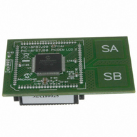
MA180025 Microchip Technology, MA180025 Datasheet - Page 297

MA180025
Manufacturer Part Number
MA180025
Description
MODULE PLUG-IN PIC18F87J90 PIM
Manufacturer
Microchip Technology
Series
PIC®r
Specifications of MA180025
Accessory Type
Plug-In Module (PIM) - PIC18F87J90
Product
Microcontroller Modules
Silicon Manufacturer
Microchip
Core Architecture
PIC
Core Sub-architecture
PIC18
Silicon Core Number
PIC18F
Silicon Family Name
PIC18FxxJxx
Lead Free Status / RoHS Status
Lead free / RoHS Compliant
For Use With/related Products
PICDEM LCD 2 Demonstration Board (DM163030)
For Use With
DM163030 - KIT DEV PICDEM LCD2
Lead Free Status / Rohs Status
Lead free / RoHS Compliant
Available stocks
Company
Part Number
Manufacturer
Quantity
Price
Company:
Part Number:
MA180025
Manufacturer:
Microchip Technology
Quantity:
135
Company:
Part Number:
MA180025
Manufacturer:
MICROCHIP
Quantity:
12 000
- Current page: 297 of 450
- Download datasheet (4Mb)
2010 Microchip Technology Inc.
21.7
The A/D Converter, in the PIC18F87J90 family of
devices, includes a self-calibration feature which com-
pensates for any offset generated within the module.
The calibration process is automated and is initiated by
setting the ADCAL bit (ADCON0<7>). The next time
the GO/DONE bit is set, the module will perform a
“dummy” conversion (that is, with reading none of the
input channels) and store the resulting value internally
to compensate for the offset. Thus, subsequent offsets
will be compensated.
The calibration process assumes that the device is in a
relatively steady-state operating condition. If A/D
calibration is used, it should be performed after each
device Reset or if there are other major changes in
operating conditions.
21.8
The selection of the automatic acquisition time and A/D
conversion clock is determined, in part, by the clock
source and frequency while in a power-managed
mode.
TABLE 21-2:
INTCON
PIR1
PIE1
IPR1
PIR3
PIE3
IPR3
ADRESH
ADRESL
ADCON0
ADCON1
ADCON2
CCP2CON
PORTA
TRISA
PORTF
TRISF
Legend:
Note 1:
Name
A/D Converter Calibration
Operation in Power-Managed
Modes
RA<7:6> and their associated latch and direction bits are configured as port pins only when the internal
oscillator is selected as the default clock source (FOSC2 Configuration bit = 0); otherwise, they are
disabled and these bits read as ‘0’.
— = unimplemented, read as ‘0’. Shaded cells are not used for A/D conversion.
GIE/GIEH PEIE/GIEL TMR0IE
TRISA7
TRIGSEL
A/D Result Register High Byte
A/D Result Register Low Byte
ADCAL
TRISF5
RA7
ADFM
Bit 7
SUMMARY OF A/D REGISTERS
RF7
—
—
—
—
—
—
—
(1)
(1)
TRISA6
TRISF4
LCDIE
LCDIP
LCDIF
RA6
ADIF
ADIE
ADIP
Bit 6
RF6
—
—
—
—
(1)
(1)
TRISA5
TRISF5
VCFG1
ACQT2
DC2B1
RC1IF
RC1IE
RC1IP
RC2IF
RC2IE
RC2IP
CHS3
Bit 5
RA5
RF5
TRISA4
TRISF4
VCFG0
ACQT1
DC2B0
INT0IE
TX1IF
TX1IE
TX1IP
TX2IF
TX2IE
TX2IP
CHS2
Bit 4
RA4
RF4
PIC18F87J90 FAMILY
CCP2M3
CTMUIF
CTMUIE
CTMUIP
TRISA3
TRISF3
If the A/D is expected to operate while the device is in
a power-managed mode, the ACQT<2:0> and
ADCS<2:0> bits in ADCON2 should be updated in
accordance with the power-managed mode clock that
will be used. After the power-managed mode is entered
(either of the power-managed Run modes), an A/D
acquisition or conversion may be started. Once an
acquisition or conversion is started, the device should
continue to be clocked by the same power-managed
mode clock source until the conversion has been com-
pleted. If desired, the device may be placed into the
corresponding power-managed Idle mode during the
conversion.
If the power-managed mode clock frequency is less
than 1 MHz, the A/D RC clock source should be
selected.
Operation in Sleep mode requires the A/D RC clock to
be selected. If bits, ACQT<2:0>, are set to ‘000’ and a
conversion is started, the conversion will be delayed
one instruction cycle to allow execution of the SLEEP
instruction and entry to Sleep mode. The IDLEN and
SCSx bits in the OSCCON register must have already
been cleared prior to starting the conversion.
PCFG3
ACQT0
SSPIF
SSPIE
SSPIP
CHS1
RBIE
Bit 3
RA3
RF3
CCP2M2
TMR0IF
CCP2IF
CCP2IE
CCP2IP
TRISA2
PCFG2
TRISF2
ADCS2
CHS0
Bit 2
RA2
RF2
—
—
—
GO/DONE
CCP2M1
TMR2IF
TMR2IE
TMR2IP
CCP1IE
CCP1IP
CCP1IF
TRISA1
TRISF1
PCFG1
ADCS1
INT0IF
Bit 1
RA1
RF1
DS39933D-page 297
CCP2M0
RTCCIE
RTCCIP
TMR1IF
TMR1IE
TMR1IP
RTCCIF
TRISA0
PCFG0
ADCS0
ADON
RBIF
Bit 0
RA0
—
—
on page
Values
Reset
59
62
62
62
62
62
62
61
61
61
61
61
64
63
62
62
62
Related parts for MA180025
Image
Part Number
Description
Manufacturer
Datasheet
Request
R

Part Number:
Description:
Manufacturer:
Microchip Technology Inc.
Datasheet:

Part Number:
Description:
Manufacturer:
Microchip Technology Inc.
Datasheet:

Part Number:
Description:
Manufacturer:
Microchip Technology Inc.
Datasheet:

Part Number:
Description:
Manufacturer:
Microchip Technology Inc.
Datasheet:

Part Number:
Description:
Manufacturer:
Microchip Technology Inc.
Datasheet:

Part Number:
Description:
Manufacturer:
Microchip Technology Inc.
Datasheet:

Part Number:
Description:
Manufacturer:
Microchip Technology Inc.
Datasheet:

Part Number:
Description:
Manufacturer:
Microchip Technology Inc.
Datasheet:


